


CMOS-Memristor Hybrid Nanoelectronics
These hybrid circuits are suitable for memory, FPGA, DSP, and analog applications.
The memristor is the fourth fundamental passive electronic device in addition to the resistor, capacitor, and inductor. By integrating with complementary metal oxide semiconductor (CMOS) devices, memristors show promise for development of revolutionary new nanoelectronic computing architectures with significantly reduced size and extremely low consumed power. The proposed effort explores a novel, high-payoff nanotechnology area that exploits crossbar nanoelectronic logic elements as well as the recently demonstrated phenomena of memristance. Specifically, the goal of this project was to explore CMOS-memristor hybrid nanoelectronic circuits for memory, FPGA, DSP, analog, and neuromorphic applications.
Crossbar computer logic architectures are complex matrices of interconnected nodes that show great promise for scalability, size, weight, and power issues. In their simplest form, crossbar junctions consist of two nanowires (less than 100-nm wide) that physically “cross” each other. The junction between these nanowires is composed of a junction material with tailored transport properties. Crossbar logic elements enable massively parallel computations with the potential for a reduction in power consumption and size by up to 2-3 orders of magnitude. Crossbar computing is also tolerant to hardware defects due to its intrinsic, network-onchip flexibility to re-route around defects.
In order to take advantage of these new memristive properties, it is necessary that memristive nanoelectronics be successfully integrated with current CMOS process technology. The electronic transport properties of memristive nanoelectronics driven by CMOS circuits will provide critical insights into subcircuit designs and subsequent advanced architectures.
The specific tasks of the project included: material selection, integration flow development, circuit design and simulation, and demonstration vehicle fabrication/testing. Materials selection and integration flow development was performed in conjunction with the CNSE Center for Semiconductor Research. Fabrication engineers were consulted for compatible back end of the line (BEOL) materials with memristive properties and vertical integration design built off of previous work at CNSE for CMOS transistor fabrication.
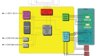
Modeling and simulation were performed using commercially available software including Verilog-A and SPICE. Novel code was written to simulate one transistor/one memristor (1T1R) devices, as well as an FPGA routing circuit utilizing memristive elements. Memristor electrical behavior was modeled as bipolar switching, based on measurements of individual memristive devices. All other device characteristics were taken from standard CMOS devices using a standard 65-nm device platform. FPGA/memristor demonstration devices were fabricated by manually connecting individual memristors with transistors using wire bonding to achieve an FPGA routing switch that could potentially replace an SRAM-based routing switch. This breadboard device was then tested in an Agilent 1500 probe station with associated analysis hardware/ software.
In this project, the design and simulation of 1T1R structures was completed. The Verilog A model was developed for memristor for SPICE simulation. Therefore, the SPICE-Verilog A simulator can be used to analyze the performance of CMOS-memristor 1T1R cells for memory applications.
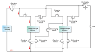
The second result obtained in this work was the design and simulation of the novel CMOS-memristor routing element. This structure can utilize two complementary memristors to control a pass transistor, providing an efficient routing element for FPGA applications. The important comparison was carried out between the simulation and the measurement of the real CMOS-memristor circuitry. The simulation was highly consistent with the measurement, which demonstrates the first measured and simulated CMOS-memristor hybrid routing circuit.
The memristive elements can be integrated with source, drain, or gate regions of buried CMOS transistors. Follow-on efforts will focus on demonstration of these hybrid structures, and electrical measurement to demonstate their utility in the simulated/modeled 1T1R and FPGA-based structures from this effort.
This effort successfully produced simulation data and code for hybrid CMOS/memristor devices. The Verilog- A and SPICE code can be used for future efforts, which could include incorporation of empirical data from device measurements. This will be critical for modeling behavior of integrated CMOS/memristor devices and ensuring that functional devices can be fabricated. The preliminary measurement data from the FPGA-routing/memristor circuits is also informative for future designs to simplify FPGA routing by incorporation of memristor elements.
This work was done by Wei Wang of the State University at Albany for the Air Force Research Laboratory. AFRL-0208
This Brief includes a Technical Support Package (TSP).
CMOS-Memristor Hybrid Nanoelectronics
(reference AFRL-0208) is currently available for download from the TSP library.
Don't have an account?
More From SAE Media Group
Tech Briefs
Silicon Carbide High-Voltage Switch
Aerospace & Defense Tech Briefs
Content Addressable Memory (CAM) Technologies for Big Data and Intelligent Electronics Enabled By Magneto-Electric Ternary CAM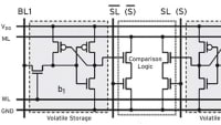

Tech Briefs
SEU-Tolerant Flip-Flops

Aerospace & Defense Tech Briefs
Magnetic Random Access Memory Integrated Passive Components
Embedded Computing INSIDER
High-Efficiency Power Amplifier Could Bring 5G Cell Phones

Tech Briefs
Reconfigurable Chaos-Based Microchips

Aerospace & Defense Tech Briefs
Low-Power Circuit for an Electromagnetic Warning System Sensor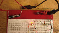

Tech Briefs
A Two-in-One Storage and Computing Device
Tech Briefs
Single Event Upset Suppression System (SEUSS)
Aerospace & Defense Tech Briefs
Energy-Filtered Tunnel Transistor: A New Device Concept Toward Extremely Low Energy Consumption Electronics

Aerospace & Defense Tech Briefs
Heterogeneous Integration Technology
Aerospace & Defense Tech Briefs
DC Power Converter for 200°C Containing SiC Transistors

Tech Briefs
5Ws of the Ultra-Thin Memory Storage Device
Tech Briefs
3D Chip Combines Computing and Data Storage

Aerospace & Defense Tech Briefs
Silicon Carbide Junction Field-Effect Transistor Devices for Scalable Solid-State Circuit Breakers

Tech Briefs
Next-Generation Computer Chip Has Two Heads
Overview
The document is a Final Technical Report titled "Complementary Metal Oxide Semiconductor (CMOS)-Memristor Hybrid Nanoelectronics," published by the Air Force Research Laboratory (AFRL) in June 2011. The report outlines a project aimed at exploring the integration of CMOS technology with memristors to develop hybrid nanoelectronic circuits suitable for various applications, including memory, field-programmable gate arrays (FPGA), digital signal processing (DSP), analog systems, and neuromorphic computing.
The project, conducted from March to November 2010, involved several key tasks: material selection, development of integration flows, circuit design and simulation, and the fabrication and testing of demonstration vehicles. The report highlights three major accomplishments:
-
Model Development: A Verilog-A model of a memristor was created, enabling co-simulation with SPICE for one transistor one memristor (1T1R) circuits and memory cells. This model is crucial for understanding the behavior of memristors in hybrid circuits.
-
Demonstration Platform Testing: Electrical measurements were conducted on a memristor-FPGA routing switch demonstration platform. The results from these measurements were compared with simulation outcomes, validating the effectiveness of the developed models and designs.
-
Integration Strategy: An integration strategy for fabricating CMOS/memristor hybrid devices was explored, laying the groundwork for future programs aimed at developing integrated devices that leverage the advantages of both technologies.
The report emphasizes the potential of CMOS-memristor hybrids to enhance performance in various electronic applications, particularly in areas requiring efficient memory and processing capabilities. The findings from this project are expected to inform follow-on research and development efforts, contributing to advancements in nanoelectronics and the broader field of computing.
Overall, the report serves as a comprehensive overview of the project's objectives, methodologies, and outcomes, providing valuable insights into the future of hybrid nanoelectronic circuits. It is approved for public release and is intended to facilitate scientific and technical information exchange within the research community and beyond.
Top Stories
INSIDERManufacturing & Prototyping
![]() How Airbus is Using w-DED to 3D Print Larger Titanium Airplane Parts
How Airbus is Using w-DED to 3D Print Larger Titanium Airplane Parts
NewsAutomotive
![]() Microvision Aquires Luminar, Plans Relationship Restoration, Multi-industry Push
Microvision Aquires Luminar, Plans Relationship Restoration, Multi-industry Push
INSIDERAerospace
![]() A Next Generation Helmet System for Navy Pilots
A Next Generation Helmet System for Navy Pilots
INSIDERDesign
![]() New Raytheon and Lockheed Martin Agreements Expand Missile Defense Production
New Raytheon and Lockheed Martin Agreements Expand Missile Defense Production
ArticlesAR/AI
![]() CES 2026: Bosch is Ready to Bring AI to Your (Likely ICE-powered) Vehicle
CES 2026: Bosch is Ready to Bring AI to Your (Likely ICE-powered) Vehicle
Road ReadyDesign
Webcasts
Semiconductors & ICs
![]() Advantages of Smart Power Distribution Unit Design for Automotive...
Advantages of Smart Power Distribution Unit Design for Automotive...
Unmanned Systems
![]() Quiet, Please: NVH Improvement Opportunities in the Early Design...
Quiet, Please: NVH Improvement Opportunities in the Early Design...
Electronics & Computers
![]() Cooling a New Generation of Aerospace and Defense Embedded...
Cooling a New Generation of Aerospace and Defense Embedded...
Power
![]() Battery Abuse Testing: Pushing to Failure
Battery Abuse Testing: Pushing to Failure
AR/AI
![]() A FREE Two-Day Event Dedicated to Connected Mobility
A FREE Two-Day Event Dedicated to Connected Mobility