


Gallium Nitride High-Power Electronics
GaN electronic devices can outperform silicon carbide devices.
Gallium nitride (GaN) high-power electronic (HPE) devices have the potential to outperform those made from 4H-silicon carbide (SiC), the polytype used for HPE devices, because it has a larger critical electric field, ξC, the field at which the device breaks down – 3.5 versus 2.5 MV/cm. This is due primarily to GaN’s larger energy gap, EG – 3.39 eV versus 3.25 eV. GaN also has a slightly larger electron mobility, μ – 930 versus 900 cm2/V·s.
The ability to form a solid solution also increases the diversity of the devices one can fabricate. An important type of device is the high electron mobility transistor (HEMT), in which a two-dimensional electron gas (2DEG) with a larger electron mobility than is found in the bulk is created at the AlGaN/GaN interface. The mobility is larger because the electrons are supplied by donors in the AlGaN, which are separated from the 2DEG so that they do not scatter the electrons as effectively. Also, the AlGaN/GaN interface can be very smooth, because the AlGaN grows epitaxially on the GaN and does not contain mismatch dislocations when its thickness is less than its critical thickness.
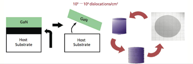
GaN device structures contain a large number of crystalline defects, most of which are dislocations created by the mismatch between the GaN film and the substrate on which it is grown. The structure is a heterostructure; that is, the film and substrate are different materials, and the difference in their lattice parameters is accommodated by the formation of misfit dislocations. Foreign substrates are required because, until very recently, large, good-quality GaN crystals have not been grown. They cannot be grown in the traditional manner because GaN sublimates at normal pressures, and the nitrogen (N2) partial pressure in equilibrium with the GaN is extraordinarily high at reasonable growth pressures. As a result, the GaN films are grown primarily on (0001) oriented sapphire (Al2O3), which has a 13% mismatch, or (0001) SiC, which has a 3.5% mismatch.
Even though the dislocation concentration is larger at the film/substrate interface, a large number of dislocations, called threading dislocations, propagate through the film. Typically, there are ~109 threading dislocations/cm2 in the GaN films grown by metal-organic chemical vapor deposition (MOCVD), and ~1010 in films grown by molecular beam epitaxy (MBE), when they are deposited on either substrate.
Devices were fabricated using the newly developed GaN substrates, and they were compared with devices made using GaN films grown on sapphire or SiC substrates. The devices being fabricated are Schottky diodes (SDs) and HEMTs, with the initial primary emphasis being on the SDs. The new substrates that are being investigated are ones being grown by hydride vapor phase epitaxy (HVPE) and ammonothermal growth.
In HVPE growth, thick GaN films are usually grown on sapphire substrates, and then the substrate is removed by rapidly heating the GaN film that absorbs light from a laser with a wavelength that is transparent to sapphire. The rapid thermal expansion of the GaN causes it to “pop off.” This thick film is then used as a substrate for growing homoepitaxial GaN films that are >1 mm thick from which wafers can be cut.
The ammonothermal crystals are grown in an autoclave containing supercritical ammonia (NH3), NH3 at pressures where the vapor cannot be distinguished from the liquid, and GaN feedstock at pressures of 0.1–0.3 GPa and relatively low temperatures of 400–600 °C. The crystals that are grown can be as large as 2" in diameter, and they have very good crystal quality. They contain only ~103 dislocations/cm2, and their x-ray rocking curve peak width can be as low as 16", compared to ~75" for the best HVPE substrates and ~200" for the best MOCVD films. In addition, they can be doped >1018 cm-3 and have a resistivity of 10-2 to 10-3 Ω·cm, which translates into a specific resistance of 0.35–0.035 mΩ· cm2 for 350 μm thick wafers.
It would be desirable to grow AlGaN on high-quality aluminum nitride (AlN) substrates in such a way that the dislocations are confined to the region of the interface, and only a few propagate up to the AlGaN surface where the devices are fabricated and/or the high electrical stress points occur. This would enable growth of AlGaN of any composition with low concentrations of dislocations for any Al content.
This work was done by Kenneth A. Jones, Timothy A. Walsh, Randy P. Tompkins, Iskander G. Batyrev, Michael A. Derenge, Kevin W. Kirchner, and Cuong B. Nguyen of the Army Research Laboratory. ARL-0128
More From SAE Media Group


Tech Briefs
Metallization for SiC Semiconductors

Electronics & Sensors INSIDER
Researchers Create First Functional Semiconductor Made from Graphene

Power Electronics INSIDER
Substrate Engineering to Improve Power Electronics
Electronics & Sensors INSIDER
Scientists Create Superconducting Semiconductor Material
Electronics & Sensors INSIDER
New Method Gives Robust Transistors

Tech Briefs
Turning Diamond into Metal
Power Electronics INSIDER
Improved GaN-Based Semiconductor Devices for Power Electronics
Electronics & Sensors INSIDER
Tiny But Mighty: Next-Gen Transistors Hold Great Promise
Electronics & Sensors INSIDER
2D Materials for Extra Thin Computer Chips


Tech Briefs
Organic Carbon-Nitride Semiconductor
Electronics & Sensors INSIDER
New Material Will Make Locally Flexible Diodes Possible
Lighting Technology
Bright Future for GaN Nanowires
Electronics & Sensors INSIDER
Advanced Microelectronics: Why A Next-Gen Semiconductor Doesn’t Fall to Pieces
Tech Briefs
Integrating Fragile 2D Materials into Devices


Electronics & Sensors INSIDER
Graphene-Based Electronics
Tech Briefs
Printing Microchip Patterns on Curvy Surfaces

Top Stories
INSIDERDefense
![]() New Raytheon and Lockheed Martin Agreements Expand Missile Defense Production
New Raytheon and Lockheed Martin Agreements Expand Missile Defense Production
NewsAutomotive
![]() Ford Announces 48-Volt Architecture for Future Electric Truck
Ford Announces 48-Volt Architecture for Future Electric Truck
INSIDERManufacturing & Prototyping
![]() Active Strake System Cuts Cruise Drag, Boosts Flight Efficiency
Active Strake System Cuts Cruise Drag, Boosts Flight Efficiency
ArticlesTransportation
![]() Accelerating Down the Road to Autonomy
Accelerating Down the Road to Autonomy
INSIDERMaterials
![]() How Airbus is Using w-DED to 3D Print Larger Titanium Airplane Parts
How Airbus is Using w-DED to 3D Print Larger Titanium Airplane Parts
Road ReadyTransportation
Webcasts
Electronics & Computers
![]() Cooling a New Generation of Aerospace and Defense Embedded...
Cooling a New Generation of Aerospace and Defense Embedded...
Power
![]() Battery Abuse Testing: Pushing to Failure
Battery Abuse Testing: Pushing to Failure
Connectivity
![]() A FREE Two-Day Event Dedicated to Connected Mobility
A FREE Two-Day Event Dedicated to Connected Mobility
Automotive
![]() Quiet, Please: NVH Improvement Opportunities in the Early Design Cycle
Quiet, Please: NVH Improvement Opportunities in the Early Design Cycle
Transportation
![]() Advantages of Smart Power Distribution Unit Design for Automotive &...
Advantages of Smart Power Distribution Unit Design for Automotive &...
Aerospace
![]() Sesame Solar's Nanogrid Tech Promises Major Gains in Drone Endurance
Sesame Solar's Nanogrid Tech Promises Major Gains in Drone Endurance