


Advances in High-Frequency PCB Materials
Traditionally, RF/microwave printed circuit board applications were developed based on the needs that came out of the military market. Applications like radar and guidance systems were operating at frequencies where traditional printed circuit board (PCB) materials like epoxy/woven glass did not have the properties — mainly tight dielectric constant control and low dielectric loss — that allowed them to be used at frequencies in the +1GHz range. Instead of PCBs, designers had to use waveguide structures as the first RF/microwave circuits; however, this meant bulky and
heavy solutions.
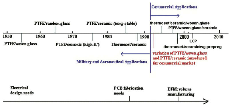
By the mid 1990s, much of the focus in this market was to find reduced-cost solutions. Tighter DoD budgets meant doing more with less, and the RF/microwave market began to be dominated by the wireless telecom market. This new market began to dictate the types of PCB materials that were being developed. In the past five years, we have begun to see a resurgence in high-frequency product development aimed at the very important defense market (see Figure 1). Advances in areas of weight, passives, and MLB techniques will be covered.
Buried Passives
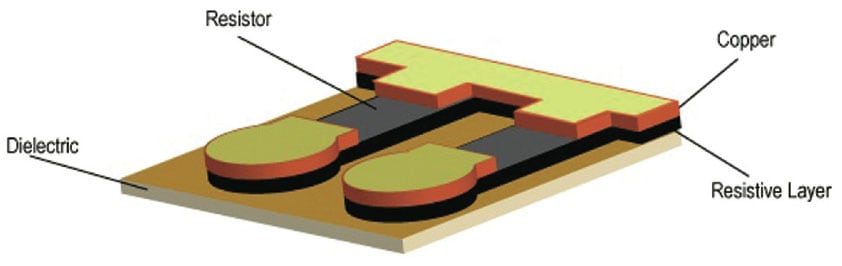
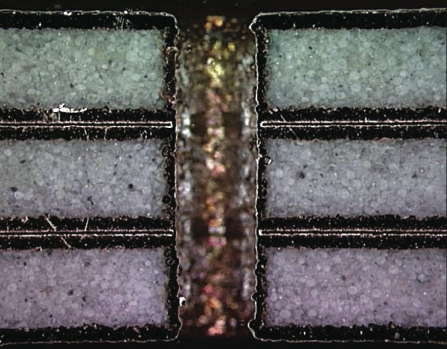
A thin resistive layer is applied to an electrodeposited copper foil. The range of values of resistors that can be achieved in high-frequency materials ranges from 25 to 50 Ohms/square and for some particular construction/ dielectric combinations, as high as 100 Ohms/square. A double etch process is required to achieve the desired resistor; the first etching process eliminates the copper on all surfaces where exposed dielectric is needed, while the second etching process is needed to expose the resistive layer at the desired length to create the needed resistor value. Figure 2 gives an example of a resistor using this technology.
These improvements allow designers to now have the ability to work with thin, temperature-stable dielectrics, achieved through the use of selected filler/resin combinations and tight dimensional tolerances (due to woven glass structures for reinforcement) in combination with resistive copper foils to achieve high-level passive integration within an MLB structure.
Lightweight PCB Materials
Most of the low-dielectric-constant, low-loss substrate materials available today have the disadvantage of having high-temperature coefficient of dielectric constant (TCDk) and high coefficient of thermal expansion (CTE) in the Z-axis. When operating in a thermal cycling environment, as are many airborne applications, designers are challenged with compensating for changes in electrical and mechanical performance of the circuit. The combination of PTFE and glass spheres allows this material to have a TCDk of 22 ppm/°C (vs. -125 ppm/°C for comparable PTFE substrates), and a CTE-Z axis of 46 ppm/°C (vs. 200 for comparable PTFE substrates). By selecting this material, the designer’s job is simplified, and changes in electrical and mechanical performance are reduced.
Improved MLB Manufacturing
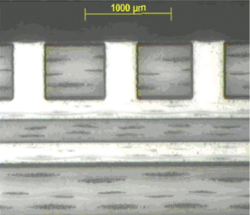
Thermoset RF materials have posed an advantage over PTFE because of their processing similarity to FR-4 and inherent lower processing costs, but limitations in design existed due to the low flow nature of the matched prepregs; in particular, fill of blind vias. Increased flow, high-frequency pre-pregs are now available. Besides having ideal RF performance, these prepregs can now be used to fill blind vias, as shown in Figure 5. RF engineers now have the flexibility to design complex MLBs with low-cost practices commonly found in the FR-4 industry.
A limitation to selecting these low-loss multilayer thermoset laminates had been that the selection of dielectric constants had been restricted to values ranging from 3 to 4. Today, that is no longer the case. We have now seen new thermoset laminates/prepregs introduced that have a dielectric constant of 6.15, and have matching higher-flow RF prepregs, expanding the material choices available for RF MLB designs. This new family of products has also given designers a second option where previously, LTCC would have been the only approach.
Conclusion
The world of high-frequency PCB materials is going through many changes, and the material choices available to designers continue to expand. Design centers are interfacing more openly with substrate suppliers in order to develop products that continue to enable further advances in technology. Successful designs require close interaction among the designer, the PCB facility, and the laminate supplier working together to continue to push the envelope of what can be achieved. This has been the trademark of the military RF/microwave market. The materials presented have unique properties and can be optimized in various ways depending on the application. When selecting a PCB material, one is also selecting a PCB material supplier. Choosing a material supplier that stands behind the products they sell and is willing to work with the customer base to further develop the next generation of materials in a timely fashion is as important as the material itself.
This article was written by Art Aguayo, Senior Market Development Manager, Advanced Circuit Materials Division, Rogers Corporation, Chandler, AZ. For more information, Click Here .
More From SAE Media Group
Aerospace & Defense Tech Briefs
Making a Material Difference in Aerospace & Defense Electronics
Aerospace & Defense Tech Briefs
Next-Generation Antenna Design
Tech Briefs
Automated Tow/Tape Placement System
Aerospace & Defense Tech Briefs
Using Thermoplastic Composites for Aerospace Applications

Aerospace & Defense Tech Briefs
Unlocking the Power of Ceramic Matrix Composites
Aerospace & Defense Tech Briefs
How Lightweight Coatings Protect Aerospace and Defense Electronics
Aerospace & Defense Tech Briefs
Additive Manufacturing Materials for RF Components
Tech Briefs
3D-Printed Composites for High-Temperature Uses
Aerospace & Defense Tech Briefs
Thermoplastic Composites to Play Enhanced Role in Next-Generation Aerospace Applications
Aerospace & Defense Tech Briefs
Advanced Multifunctional Materials for High Speed Combatant Hulls
Aerospace & Defense Tech Briefs
Fiber-Reinforced Thermoplastic Composites
Aerospace & Defense Tech Briefs
Biobased Carbon Fibers and Thermosetting Resins for Use in DOD Composites Applications
Aerospace & Defense Tech Briefs
High Temperature Graphene-Peek Adhesive
Aerospace & Defense Tech Briefs
Molded RF Materials for Hypersonic Sensors and Seekers
Aerospace & Defense Tech Briefs
Biobased Carbon Fibers and Thermosetting Resins for Use in DOD Composites Applications
Aerospace & Defense Tech Briefs
Taming the Thermal Behavior of Solid-State Military Lasers

Aerospace & Defense Tech Briefs
Design Guidelines for Military and Aerospace PCBs
Aerospace & Defense Tech Briefs
Specifying Components for Space Applications
Aerospace & Defense Tech Briefs
Fiber Computer Allows Apparel to Run Apps and Understand the Wearer

Aerospace & Defense Tech Briefs
Towards Sustainable Recycling of Epoxy-Based Polymers: Approaches and Challenges of Epoxy Biodegradation

Tech Briefs
Silicon Carbide Fiber Tows
Aerospace Manufacturing and Machining INSIDER
Can This Self-Healing Composite Make Airplane and Spacecraft Components Last for Centuries?
Tech Briefs
Electronics Withstand Extreme Heat
Aerospace & Defense Tech Briefs
Testing EMI Materials for Battlefield Applications
Top Stories
NewsSensors/Data Acquisition
![]() Microvision Aquires Luminar, Plans Relationship Restoration, Multi-industry Push
Microvision Aquires Luminar, Plans Relationship Restoration, Multi-industry Push
INSIDERRF & Microwave Electronics
![]() A Next Generation Helmet System for Navy Pilots
A Next Generation Helmet System for Navy Pilots
INSIDERWeapons Systems
![]() New Raytheon and Lockheed Martin Agreements Expand Missile Defense Production
New Raytheon and Lockheed Martin Agreements Expand Missile Defense Production
NewsAutomotive
![]() Ford Announces 48-Volt Architecture for Future Electric Truck
Ford Announces 48-Volt Architecture for Future Electric Truck
INSIDERAerospace
![]() Active Strake System Cuts Cruise Drag, Boosts Flight Efficiency
Active Strake System Cuts Cruise Drag, Boosts Flight Efficiency
ArticlesTransportation
Webcasts
Aerospace
![]() Cooling a New Generation of Aerospace and Defense Embedded...
Cooling a New Generation of Aerospace and Defense Embedded...
Energy
![]() Battery Abuse Testing: Pushing to Failure
Battery Abuse Testing: Pushing to Failure
Power
![]() A FREE Two-Day Event Dedicated to Connected Mobility
A FREE Two-Day Event Dedicated to Connected Mobility
Automotive
![]() Quiet, Please: NVH Improvement Opportunities in the Early Design Cycle
Quiet, Please: NVH Improvement Opportunities in the Early Design Cycle
Electronics & Computers
![]() Advantages of Smart Power Distribution Unit Design for Automotive &...
Advantages of Smart Power Distribution Unit Design for Automotive &...
Unmanned Systems
![]() Sesame Solar's Nanogrid Tech Promises Major Gains in Drone Endurance
Sesame Solar's Nanogrid Tech Promises Major Gains in Drone Endurance