Benefits and Challenges of Direct-RF Sampling for Avionic Platforms

Recent advances in the operation of advanced CMOS processes for extremely high-speed and high dynamic range analog-to-digital (ADC) and digital-to-analog (DAC) data converters has led to their use in directly sampling microwave and even millimeter wave signals. Typically, in these applications, minimal pre or post-conditioning stages separate the ADCs and DACs from the antenna or, for Active Electronically Steered Arrays (AESA) antenna elements. This results in an extremely compact and flexible system solution and this has enabled a generation of fully digital phased arrays that are capable of being dynamically reconfigured to perform a multitude of functions.
History and Enabling Technologies
High-speed data converter devices in the past, those exceeding roughly 3 GS/s, were largely realized using semiconductor technologies that were rather specialized for use in mixed-signal analog/digital applications. These processes typically used bipolar transistors and were formed using either GaAs HBT, silicon, or silicon germanium processes. Due to the limited integration capability of these processes and their relatively high power consumption and cost, the resolution of these converters were generally limited to approximately eight bits, and sample rates rarely exceeded 10 GS/s. The architectures for the ADCs of this generation were typically flash while the DACs were implemented with current-mode designs. Neither the ADCs nor DACs were time-interleaved for the vast majority of applications, though using this approach to increase sample rates became more common in test equipment applications where the cost, board space, power consumption, and frequent calibration of their associated time-interleaving errors could be managed. Higher resolution ADCs, those at or exceeding 12 bits, with medium sampling rates in the range of 10 to 3,000 MS/s were constructed using a pipeline architecture in which a cascade of analog stages is used, with intermediate quantization results being developed as the intermediate analog residual error values propagate through the converter stages.

Since approximately 2010, Successive Approximation Register (SAR) ADCs have become increasingly used for high-speed converters at rates from under 1 MS/s to as high as 1 GS/s. The resolution of these devices is typically limited to 12 bits. In particular, asynchronous time-interleaved (TI) SAR ADCs have been developed at rates as high as 256 GS/s and resolutions of 6 to 10 bits for fiber optic modems in the optical transport market. These extremely high-speed ADCs, and their associated DACs, which typically operate at similar speeds, are implemented in some of the most advanced bulk or FinFET CMOS processes since the vast amount of data they produce must be processed locally on-chip. The efficiency, as measured by the Walden figure of merit, for these data converters has progressed from approximately 1 picojoule per conversion step (pJ/c-step) to roughly 0.01 pJ/c-step over the course of the last 13 years (Murmann, 2023). The effective number of bits (ENOB) for these devices range from about 4.8 bits to as high as 8.2 bits. While this may not sound like such a high value, when considering the extremely high sampling rate, the input-referred noise power spectral density of an ADC having an ENOB of 8 and a sampling rate of 50 GS/s is -154 dBFS/Hz. With a typical input loading level at full-scale of -3 dBm this input referred NSD becomes -157 dBm/Hz and the equivalent noise figure is 17 dB. This, together with their very low harmonic distortion and excellent spur free dynamic range (SFDR) performance, result in an extremely good receiver front-end. Such a device may have a first-Nyquist zone extending all the way to 20 GHz, or well into V-band with more recent advances. For comparison, a converter at 3 GS/s would require a raw resolution of between 12 and 14 bits to meet this performance level.

So, in approximately 13 years, the combined advances in semiconductor technology and data converter architecture have led to an increase in conversion rate of nearly two orders of magnitude, and approximately the same increase in converter efficiency. It is interesting to note that this has roughly tracked Moore’s Law. It is also interesting to see that, architecturally, what has enabled this is massive parallelism: Many data converters operating at lower rates that are time-interleaved to achieve extremely high overall conversion rates. This is a clear trend going forward, not only in ADCs but in systems architectures, and we will see later in this article that it enables rather astounding performance levels to be achieved. Examples of the performance of this ADC technology are shown in Figures 1 and 2.

Resulting Digital RF System Architecture and Benefits
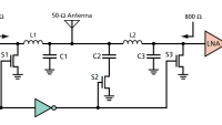
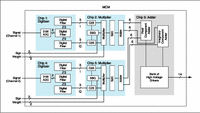
The architecture for such a “digital RF” transceiver is shown in Figure 3 and consists of the antenna element followed by a transmit/receive (T/R) switch, to which is coupled a low noise amplifier (LNA) for the receive path and a power amplifier (PA) for the transmit path. These three devices are often realized in a suitable process such as SiGe, RF-SOI CMOS, GaAs, or GaN. These will frequently interface to some level of filtering and gain control, and sometimes a switched filter bank, before the digital RF transceiver.
Note that this architecture eliminates the RF mixer in both the receive and transmit paths and its associated local oscillator, thus saving large amounts of power consumption, board area, and reducing the associated nonlinearity and spurious mechanisms. The frequency tuning becomes entirely digital, using numerically controlled oscillators (NCO’s), thus achieving the ability to rapidly and precisely change the tuned frequency within a cycle of the digital logic speed. This results in precise nanosecond-level tuning with virtually no settling time.
The required die area, in 12 nm FinFET CMOS, for a digital-RF transceiver capable of a 32 GHz nyquist zone and having the level of performance described previously is under 10 mm2. Furthermore, many channels of this type can be integrated into such a device process while still maintaining excellent production yield: 32 channels of this type of device may be realized on a single die to enable a sixteen element building block for a dual-polarized digital AESA to be realized, along with the digital processing required for frequency conversion, equalization, and beam-forming. With on-chip sample clock synthesis, using synthesizers having additive aperture jitter values of under 40 femtoseconds rms, enables fully integrated solutions in which the system integrator only needs to supply a clean L-band or S-band reference clock.
Because many of the error mechanisms in such a multi-channel implementation are uncorrelated from channel-to-channel and, therefore element-to-element in the digital AESA system, the dynamic range associated with these error terms improves by the array gain factor of 10log10(N), where N is the number of antenna elements in the AESA. For a modestly sized AESA system of 1,000 elements, this improvement factor is a massive 30 dB. Note that this improvement factor is not achieved for an RF beamformed system, on boresight, for many error terms as all of the signal information flows into a single ADC.
Further improvements in performance are possible through the use of digital equalization, both linear and nonlinear, as well as through both factory-level and background calibration. This doorway to using the digital logic to improve the RF performance has been opened through co-designing the RF, mixed-signal, and DSP in an advanced CMOS node. The power consumption and die area may be impacted minimally through the addition of these features in these modern CMOS processes.
Deployable Direct-RF COTS Solution

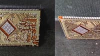
An example of a commercial application of this technology is shown in Figure 4. Annapolis Micro Systems has integrated Jariet Technologies’ Electra-MA transceiver into the DME1 ADC & DAC Card. It’s the industry’s first COTS product to ship that features 64 GS/s, 10-bit ADC and DAC Direct-RF sampling capability. The SOSA-aligned Card is targeted at demanding applications requiring direct sampling frequency coverage anywhere from 0.1 to 36 GHz (VHF through Ka-band), and/or wide instantaneous bandwidths. It’s first deployment is in a mission-critical airborne electronic warfare (EW) program.
References
- B. Murmann , “ADC Performance Survey 1997-2023,” [Online].
This article was written by Craig Hornbuckle, Chief Technology Officer, Jariet Technologies. For more information, visit www.jariettech.com .
Top Stories
INSIDERManufacturing & Prototyping
![]() How Airbus is Using w-DED to 3D Print Larger Titanium Airplane Parts
How Airbus is Using w-DED to 3D Print Larger Titanium Airplane Parts
NewsAutomotive
![]() Microvision Aquires Luminar, Plans Relationship Restoration, Multi-industry Push
Microvision Aquires Luminar, Plans Relationship Restoration, Multi-industry Push
INSIDERAerospace
![]() A Next Generation Helmet System for Navy Pilots
A Next Generation Helmet System for Navy Pilots
INSIDERDesign
![]() New Raytheon and Lockheed Martin Agreements Expand Missile Defense Production
New Raytheon and Lockheed Martin Agreements Expand Missile Defense Production
ArticlesAR/AI
![]() CES 2026: Bosch is Ready to Bring AI to Your (Likely ICE-powered) Vehicle
CES 2026: Bosch is Ready to Bring AI to Your (Likely ICE-powered) Vehicle
Road ReadyDesign
Webcasts
Semiconductors & ICs
![]() Advantages of Smart Power Distribution Unit Design for Automotive...
Advantages of Smart Power Distribution Unit Design for Automotive...
Unmanned Systems
![]() Quiet, Please: NVH Improvement Opportunities in the Early Design...
Quiet, Please: NVH Improvement Opportunities in the Early Design...
Electronics & Computers
![]() Cooling a New Generation of Aerospace and Defense Embedded...
Cooling a New Generation of Aerospace and Defense Embedded...
Power
![]() Battery Abuse Testing: Pushing to Failure
Battery Abuse Testing: Pushing to Failure
AR/AI
![]() A FREE Two-Day Event Dedicated to Connected Mobility
A FREE Two-Day Event Dedicated to Connected Mobility
