


Surviving The Embedded Design Thermo-Mechanical Envelope
The Embedded usage model is characterized as one that is operated at the extremes of available performance. Knowing that the targets of the thermal design power usage mode are only partially applicable, embedded designers must satisfy the customers’ innate desires for maximum throughput and level of service at the edges of a constrained thermo- mechanical environment.
While the mechanical envelope must handle the physical form factor and the necessary interconnects, mechanical stress must also be considered. From the MIL-STD-801F guidelines, four operational tests present challenges that exceed the shipping and handling stresses imposed by Method 514.5 of the same standard. These requirements, when superimposed upon the thermal aspects, create a formidable challenge for any SBC and peripheral mix.
The Computation Power Function
The process of electronic computation pushes electrons from place to place over resistive connections and internal devices that consume electrical potential, converting it to thermal energy as a byproduct of operation at a conversion rate that approaches 100%. Interconnects can transmit some energy out of the system and to a receiver, but the transmitted energy of an RS-422 or 232 interlink is infinitesimal compared to the thermal output of a CPU or GPU. Ethernet and optical interfaces are less efficient, as they consume significant power in the physical interface (PHY) before producing a waveform with mere milliwatts of energy. Such bi-directional communications dissipate received energy, often offsetting transmitted power. The exception to this rule is powered USB, which can consume and transmit ≥2.5W per port to an external peripheral with low loss, and therefore must be considered in design of the input power channel. Only the energy transmission losses will add to the thermal profile.
Practical power dissipation methodologies consider the total system input power as the total thermal output of the system, regardless of transmitted waveform energies. It is for this reason that efforts at CPU power reduction are at the center of low-power designs. Such an approach also includes the inefficiencies that exist in the numerous DC/DC converters ubiquitous on modern designs that regularly produce and regulate half a dozen voltage rails, all derived from a traditional 5V supply. High current CPU and GPU power subsystems may require input power at a higher potential to combat delivery and distribution losses, at the expense of converter efficiency.
Design Strategies and Constraints

Keeping semiconductor devices cool is a key to managing the negative temperature coefficient of silicon, and helps meet performance constraints. Compared to an onboard passive/radiative thermal solution, a small, lightweight heatsink and fan combination usually reduces system power consumption by more than the electrical load of the fan itself. Conduction cooling methods trade increased system mass for power reduction, improved service interval and greater overall reliability by elimination of frictional wear and contamination.
High-power CPU and support chips make holistic board cooling impractical, requiring an external thermal pathway. The method of attachment for such a thermal pathway should be considered at the same time that mechanical mounting holes and board topology are defined. A thermal attachment point may be problematic because it interferes with high-speed chip-to-chip interconnects, yet may be mitigated by judicious routing. Incorporation of thermal attachment points after layout and routing can be highly problematic unless only adhesive solutions are under consideration.
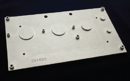
Internal thermal structures within the circuit card, normally designed to enhance device-to-board thermal transfer, can be exploited. Any conceivable structure, from a multilayer internal heat spreader to repetitive stitching of thermal attach points to ground planes can be leveraged (Figure 3). Excess capacity in the cooling pathway of high power devices helps to reduce board temperature through reversal of the thermal transfer of any enhanced device-to-board thermal pathway, allowing energy from nearby components to be dissipated through the cooled device.
When the environmental envelope precludes the use of mechanical forced convection, a thermal pathway from the source to the outer surface of the enclosure is necessary to satisfy the thermal aspects of the operational envelope. Minimizing the temperature differential across each thermal interface is highly desirable, to the point that rugged design solutions will incorporate mechanical and thermal mounting into a single metal structure that may also function as the chassis wall. While this eliminates a thermal interface, it may not be truly necessary or desired. Large output areas and attachment pressure greatly reduce the thermal differential required to transfer the requisite energy, and provide an opportunity to electrically isolate the thermal attachment. It is not uncommon for low resistance connections to DC-ground to occur from either the thermal attachment to the board or to passivated die paddles in FCBGA (Flip Chip Ball Grid Array) and will conduct to a thermal solution if chipped, cracked or damaged.
Simplified Thermal Design
Consider the Intel Dothan 1.4GHz CPU in an exposed flip-chip package. The area of the passivated silicon die (0.490" × 0.275") is approximately 0.13475in2 and represents the maximal window through which heat will flow into a receiving material. The diagonal dimension of the oblong die is just under 0.562" requiring a circular thermal pick-up of at least this diameter in order to make full contact with the exposed die paddle. The choice of material in contact with the die will influence the performance characteristics of the thermal solution. For example, 11000 Copper (388 W·°K-1·m-1) will conduct >230% more heat per unit area than 6061-T6 Aluminum (167 W·°K-1·m-1).
If a copper interface were utilized to pick up thermal energy from a Dothan CPU, and this copper were interference-fit into an aluminum spreader, what thickness of aluminum must be fit to the copper slug to produce 100% thermal transfer from the copper pickup to the aluminum carrier?
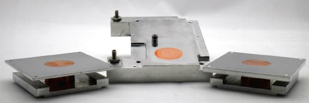
Interference-fit copper and aluminum creates very high contact pressures and a nearly ideal transfer situation occurs. Geometry suggests that when the area of the right-hand contact cylinder approaches 230% of the input area, that full thermal transfer will occur, and that beyond this there is no substantial gain in the performance of the solution. To examine this hypothesis, test jigs were constructed using 0.735" diameter 110 alloy copper and 6061 aluminum, and compared to a fully-plugged and co-milled construction of the same material (Figure 4).
Testing was performed by using the same integrated fan-sink unit on all three solutions, connected to a control unit based on an Intel Pentium-M 738 CPU, and driven by Intel’s Dothan MaxPower tool. A phase change thermal interface compound was used between the jig and the integrated fan-sink, and a micronized silver interface compound was used between the die paddle and jig.
In situations where a heat-spreader is in contact with an external case, the required case thickness is a function of the input material and area. Using the 0.13475in2 Dothan example, a 6061 aluminum spreader with output dimensions of approximately 3.50" × 1.88", the 10.76" perimeter achieves 100% of input contact at 0.0125" material thickness when the contact outline is propagated through a 6061 aluminum case wall. Standard 1⁄16" material exceeds this critical thickness by >450%. Large diameter fasteners in such a brick improve contact pressure and provide an opportunity for electrical isolation, if necessary, using thermal compound treated insulating sheets and insulating washers similar to that which is used for TO-3 style power devices.
Enhancements and Benefits
While it may be possible to design thermal interfaces and solutions for the average power case, absence of a thermal reservoir to store the excess energy until it can be effectively dissipated will limit the operational performance of the system. Designing the thermal pathways and solutions to accommodate full power operation will ultimately allow the end user to fully consume all available CPU capacity. This brings home the need to consider all power conservation methods, which begin by adopting the lowest power, widest temperature range components available.
A final electrical enhancement is to minimize the strength of pull-up resistors in the design, reducing quiescent and active currents to the minimum necessary while maintaining required signal integrity across the operational temperature range. Such an optimization may seem inconsequential individually, but when applied across buses and active-low, open drain driven signals, the total reduction power consumption, and associated thermal output, differentiates seemingly identical implementations from one another.
Summary
Modern high-density packages often result in limits on the service model, reducing the options for component-level service and repair. Customer requirements and adhesive enhancement result in similar constraints, such that the service model becomes one of board-level replacement. Adhesive enhancement improves the component-to- board thermal pathway and when coupled with precision thermal interface, aids in the control of thermal stress. The final result is greater delivered reliability with a lower total cost of ownership.
This article was written by Martin Mayer, Department Head, Research and Development, ADL Embedded Solutions (San Diego, CA). For more information, Click Here " target="_blank" rel="noopener noreferrer">http://info.hotims.com/34459-500.
More From SAE Media Group
Aerospace & Defense Tech Briefs
Simplifying Power Design with Modular Architectures
Aerospace & Defense Tech Briefs
Taming the Thermal Behavior of Solid-State Military Lasers

Aerospace & Defense Tech Briefs
Thermal Conductivity Measurement Setup for Low-Temperature Characterization of Laser Materials
Aerospace & Defense Tech Briefs
Design Guidelines for Military and Aerospace PCBs
Aerospace & Defense Tech Briefs
Trends in Military System Thermal Management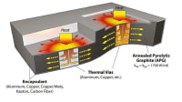
Aerospace & Defense Tech Briefs
Designing Transportable, High-Performance AI Systems for the Rugged Edge
Tech Briefs
Generating Electrical Power from Waste Heat
Aerospace & Defense Tech Briefs
Minimizing Thermal Resistance with Direct Attach Heat Spreaders
Aerospace & Defense Tech Briefs
Designing Battery Packs for Harsh Environment Mission-Critical Devices
Aerospace & Defense Tech Briefs
Designing Thermal Management Systems for Smaller, Lighter Avionics
Aerospace & Defense Tech Briefs
Using Polyimide In 3D Thin Film Multilayer Circuitry
Aerospace & Defense Tech Briefs
New 3D Chips Could Make Electronics Faster and More Energy-Efficient
Aerospace & Defense Tech Briefs
Fiber Computer Allows Apparel to Run Apps and Understand the Wearer
Aerospace & Defense Tech Briefs
Thermal Management Techniques in Avionics Cooling
Aerospace & Defense Tech Briefs
Energy-Filtered Tunnel Transistor: A New Device Concept Toward Extremely Low Energy Consumption Electronics

Tech Briefs
Ruthenium-Doped Thermoelectric Materials
Tech Briefs
Electronics Withstand Extreme Heat
Aerospace & Defense Tech Briefs
Thermal Ground Planes Optimizing Heat Transfer in Aerospace and Defense Applications
Aerospace & Defense Tech Briefs
The Tug-of-War Between Speed and Strength
Aerospace & Defense Tech Briefs
GaN Breaks Barriers

Tech Briefs
Products of Tomorrow
Aerospace & Defense Tech Briefs
New Technologies Tackle UAV Challenges
Aerospace & Defense Tech Briefs
Testing Military-Grade Adhesive in Extreme Loading Conditions
Electronics & Sensors INSIDER
MIT Team Takes a Major Step Toward Fully 3D-Printed Active Electronics
Tech Briefs
Hybrid Transformer
Aerospace INSIDER
New Power Module Developed for Next Gen Military Airborne Electronics
Aerospace & Defense Tech Briefs
Using SWaP-C Reductions to Improve UAS/UGV Mission Capabilities
Top Stories
INSIDERManufacturing & Prototyping
![]() How Airbus is Using w-DED to 3D Print Larger Titanium Airplane Parts
How Airbus is Using w-DED to 3D Print Larger Titanium Airplane Parts
INSIDERManned Systems
![]() FAA to Replace Aging Network of Ground-Based Radars
FAA to Replace Aging Network of Ground-Based Radars
NewsTransportation
![]() CES 2026: Bosch is Ready to Bring AI to Your (Likely ICE-powered) Vehicle
CES 2026: Bosch is Ready to Bring AI to Your (Likely ICE-powered) Vehicle
NewsSoftware
![]() Accelerating Down the Road to Autonomy
Accelerating Down the Road to Autonomy
EditorialDesign
![]() DarkSky One Wants to Make the World a Darker Place
DarkSky One Wants to Make the World a Darker Place
INSIDERMaterials
![]() Can This Self-Healing Composite Make Airplane and Spacecraft Components Last...
Can This Self-Healing Composite Make Airplane and Spacecraft Components Last...
Webcasts
Defense
![]() How Sift's Unified Observability Platform Accelerates Drone Innovation
How Sift's Unified Observability Platform Accelerates Drone Innovation
Automotive
![]() E/E Architecture Redefined: Building Smarter, Safer, and Scalable...
E/E Architecture Redefined: Building Smarter, Safer, and Scalable...
Power
![]() Hydrogen Engines Are Heating Up for Heavy Duty
Hydrogen Engines Are Heating Up for Heavy Duty
Electronics & Computers
![]() Advantages of Smart Power Distribution Unit Design for Automotive...
Advantages of Smart Power Distribution Unit Design for Automotive...
Unmanned Systems
![]() Quiet, Please: NVH Improvement Opportunities in the Early Design...
Quiet, Please: NVH Improvement Opportunities in the Early Design...