


Photonic Recirculating Delay Line for Analog-to-Digital Conversion
This approach modifies an analog fiber-optic link with a recirculating optical loop.
Aconventional analog fiber-optic link can be augmented with a recirculating optical delay loop so as to realize an optically assisted analogto- digital converter (ADC) that provides improved performance in terms of both speed and resolution using one (slower) electronic ADC (see figure). The overall architecture readily integrates with any electronic ADC system. Moreover, the highspeed ADC performance is fundamentally limited by the performance of the fiber-optic link. The system was constructed on an optical bench. A 1,550-nm, 50-mw diode laser was used as the optical source. The link was modulated using an 18 GHz - LiNbO3 Mach- Zehnder modulator electrically driven with a 1-GHz tone burst. The RFmodulated optical signal was injected into the recirculating delay loop via 3-dB coupler. A loop time delay of roughly 100 nanoseconds was achieved using approximately 22 meters of single mode fiber with fine time delay adjustment (+3 nanoseconds) obtained from a variable delay line. The fundamental ring architecture with unity gain is essentially a laser.
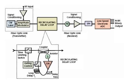
A concern involves the gain dynamics of the loop’s optical amplifier. With little or no light entering the amplifier when the loop gate is open, the turn-on time of the SOA when the light does enter will prevent the total required loop gain from being present when needed. This effect is mitigated by using distributed amplification in the loop. Two optical amplifiers were used in the loop, which allowed for a lower gain in each amplifier and thus a faster turn-on time. Future implementation of the system would perhaps use either more amplifiers or else a continuously distributed amplification scheme.
Upon exiting the loop via the 3-dB coupler, the signal is directed to a 20- GHz PIN photodetector, and the resulting periodic signal is viewed on a highspeed oscilloscope. Since the system was constructed with (connectorized) bulk optical components, this resulted in reduced SNR performance.
This work was done by Henry Zmuda of the University of Florida; Jared Pawloski of the State University of New York, Binghamton; Kristina Norelli of Syracuse University; and Michael Fanto and Thomas McEwen of the Air Force Research Laboratory. For more information, download the Technical Support Package (free white paper) at www.defensetechbriefs.com/tsp under the Photonics category. AFRL-0125
This Brief includes a Technical Support Package (TSP).

Photonic Recirculating Delay Line for Analog-to-Digital Conversion
(reference AFRL-0125) is currently available for download from the TSP library.
Don't have an account?
More From SAE Media Group
Aerospace & Defense Tech Briefs
Analysis of Analog Photonic Links Employing Multiple-Channel (Arrayed) Receivers
Aerospace & Defense Tech Briefs
Photonic Analog-to-Digital Converters
Aerospace & Defense Tech Briefs
Heterodyne RF/Optical Links Utilizing Integrated Photonics
Tech Briefs
Sensitive Optical Receivers for Space
Aerospace & Defense Tech Briefs
Stimulated Brillouin Scattering (SBS) Suppression and Long Delivery Fibers at the Multikilowatt Level with Chirped Seed Lasers
Photonics & Imaging Technology
Photonics-Based Wireless Link Breaks Speed Records for Data Transmission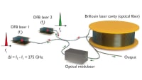
Aerospace & Defense Tech Briefs
Effect of Laser Noise on an Analog RF/Photonic Link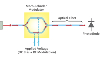

Photonics Tech Briefs
A High-Repetition-Rate Optical Communications Source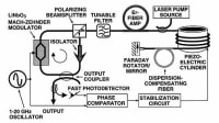
Photonics & Imaging Technology
Ultra-Broadband Photonic Chip Boosts Optical Signals
Photonics & Imaging Technology
Optical Signal Amplifying Technique
Photonics Tech Briefs
Fiber-Optic Phase-Locked Loop Sensitive to Local Strain Only
Photonics Tech Briefs
Closed-Loop Microsphere Laser for Optoelectronic Oscillator
Photonics Tech Briefs
Stabilizing Microwave Frequency of a Photonic Oscillator
Tech Briefs
Free-Space Fiber Optic Laser Rod
Aerospace & Defense Tech Briefs
Apparatus Generates CE-Phase-Stable Two-Cycle Optical Pulses
Photonics & Imaging Technology
Photonic Microwave Generation Using On-Chip Optical Frequency Combs
Aerospace & Defense Tech Briefs
BC VCSELs for RF/Photonic Links
Aerospace & Defense Tech Briefs
Everyday Life, Improved by Light: GRYPHON’s Photonic Discoveries
Photonics & Imaging Technology
Photonic Integrated Circuit Testing: Accelerating R&D From Lab to Fab
Tech Briefs
Fast-Tunable Laser SystemPhotonics & Imaging Technology
A Laser That Could Reshape the Landscape of Integrated Photonics
Photonics Tech Briefs
Fiber Laser Amplifiers with Broad Applications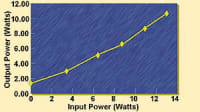
Photonics & Imaging Technology
Using Magnets to Toggle Nanolasers Leads to Better Photonics
Photonics Tech Briefs
Stabilized Fiber-Optic Distribution of Reference Frequency
Photonics Tech Briefs
OEOs With Carrier Suppression for Reduction of Phase Noise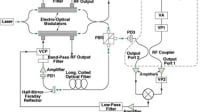
Photonics Tech Briefs
Automatic Alignment of Displacement-Measuring Interferometer
Photonics Tech Briefs
Control Program and Optical Improvements of Fresnel Microspectrometer
Photonics Tech Briefs
Frequency-Converting Photonic Link With BSSA Amplification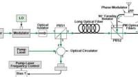
Overview
The document presents a conference paper detailing a novel approach to high-speed, high-resolution Analog-to-Digital Conversion (ADC) using a photonic recirculating delay line. The authors, Henry Zmuda, Michael Fanto, Thomas McEwen, Jared Pawloski, and Kristina Norelli, explore how this technology modifies an analog fiber optic link to enable the digitization of multi-gigahertz microwave signals with a resolution exceeding 10 effective bits.
The core concept involves utilizing a recirculating optical loop to store time-limited microwave signals, which allows for their subsequent digitization by slower, conventional electronic ADCs. This method addresses the challenges associated with high-speed signal processing, particularly the limitations imposed by the effective number of bits (ENOB) and the dynamic range of the system. The paper emphasizes that the performance of ADCs is not solely determined by conversion speed but also significantly influenced by factors such as signal-to-noise ratio (SNR) and intermodulation products introduced by modulator nonlinearities.
Key findings include the establishment of a relationship between SNR and ENOB, where the SNR is derived from the ratio of the full-scale voltage to the noise voltage. The authors provide analytical insights into the dynamic range and noise figure, demonstrating that under optimal conditions, the degradation of microwave signals is minimal, thus facilitating effective digitization.
The paper also discusses the technical requirements for achieving high ENOB, including the need for precise timing accuracy and low aperture uncertainty. For instance, a 10-bit, 10 Giga-sample per second ADC necessitates an aperture uncertainty of approximately 65 femtoseconds, a challenging requirement that can be met using advanced clocking systems like mode-locked lasers.
Experimental results are presented to support the theoretical analysis, showcasing the practical viability of the proposed system. The findings indicate that the photonic recirculating delay line can effectively enhance the performance of ADCs in high-speed applications, making it a promising solution for future developments in microwave photonics and optical signal processing.
In summary, this document outlines a significant advancement in ADC technology, highlighting the potential of photonic systems to overcome traditional limitations and improve the resolution and speed of signal digitization.
Top Stories
NewsRF & Microwave Electronics
![]() Microvision Aquires Luminar, Plans Relationship Restoration, Multi-industry Push
Microvision Aquires Luminar, Plans Relationship Restoration, Multi-industry Push
INSIDERAerospace
![]() A Next Generation Helmet System for Navy Pilots
A Next Generation Helmet System for Navy Pilots
INSIDERDesign
![]() New Raytheon and Lockheed Martin Agreements Expand Missile Defense Production
New Raytheon and Lockheed Martin Agreements Expand Missile Defense Production
INSIDERMaterials
![]() How Airbus is Using w-DED to 3D Print Larger Titanium Airplane Parts
How Airbus is Using w-DED to 3D Print Larger Titanium Airplane Parts
NewsPower
![]() Ford Announces 48-Volt Architecture for Future Electric Truck
Ford Announces 48-Volt Architecture for Future Electric Truck
ArticlesAR/AI
Webcasts
Electronics & Computers
![]() Cooling a New Generation of Aerospace and Defense Embedded...
Cooling a New Generation of Aerospace and Defense Embedded...
Automotive
![]() Battery Abuse Testing: Pushing to Failure
Battery Abuse Testing: Pushing to Failure
Power
![]() A FREE Two-Day Event Dedicated to Connected Mobility
A FREE Two-Day Event Dedicated to Connected Mobility
Unmanned Systems
![]() Quiet, Please: NVH Improvement Opportunities in the Early Design Cycle
Quiet, Please: NVH Improvement Opportunities in the Early Design Cycle
Automotive
![]() Advantages of Smart Power Distribution Unit Design for Automotive &...
Advantages of Smart Power Distribution Unit Design for Automotive &...
Energy
![]() Sesame Solar's Nanogrid Tech Promises Major Gains in Drone Endurance
Sesame Solar's Nanogrid Tech Promises Major Gains in Drone Endurance