Magnetic Memory Devices for Embedded Computing
These devices could be utilized in novel, energy-efficient, radiation-hard electronics.
A program of research has been dedicated to the development of magnetic memory devices than can be incorporated into complementary metal oxide/semiconductor (CMOS) integrated circuits, wherein these devices can be made to function as radiation- hard logic elements and as components of small random-access memories. The goal of this development was not to provide for large-scale, bulk memories, but, instead, to provide for latches and flip-flops that can serve as state and data registers for sequential logic and as configuration registers for configurable logic. A major benefit afforded by these devices is the ability to retain the logical state of a subsystem that contains the devices when turning off the power to that subsystem to save energy until operation of the subsystem is required. The subsystem can then be powered up and begin operating within a time of the order of milliseconds.

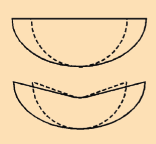
The free magnetic layers in the MTJ cells developed in this program have shapes belonging to a patented class of shapes denoted generally and informally by the term "PacMan" because of their resemblance to a character in the popular video game "Pac-Man" (see Figure 2). Through experimentation, these shapes were chosen, along with sizes and material compositions, to obtain magnetic and electric properties superior to those imparted by prior MTJ shapes. Desirable properties include high selectivity for addressing individual cells, high reading and writing speeds, large changes in resistance, long lifetimes as measured in numbers of switching cycles, narrow distributions of switching magnetic fields and associated writing electric currents, thermal stability, and small cell-to-cell differences in the aforementioned properties. The cell designs developed in this program lead to high repeatability and high fabrication yield, making it possible to design circuits to generate the necessary switching magnetic fields predictably and reliably.
Thus far, two types of data-storage circuits incorporating magnetic memory devices of this type have been designed: a differential magnetic flip-flop and a magnetic flip-flop that could be used as a shadow random-access memory. Integration of the fabrication of MTJ cells into a CMOS-integrated-circuit-fabrication process has proved elusive because of difficulties in creating metal surfaces smooth enough to accept the cells. It will be necessary to overcome this difficulty in order to carry out the next phases of the research — to develop accurate computational models of the electronic circuitry, to implement a one-wire writing scheme that is a common feature of the designs of the flip-flop circuits mentioned above, and finally, to integrate MTJ cells with CMOS circuitry.
This work was done by Gregory W. Donohoe and Kenneth Joseph Hass of the University of Idaho for the Air Force Research Laboratory.
AFRL-0076
This Brief includes a Technical Support Package (TSP).
Magnetic Memory Devices for Embedded Computing
(reference AFRL-0076) is currently available for download from the TSP library.
Don't have an account?
Overview
The document is a dissertation by Kenneth Joseph Hass, submitted for a Doctor of Philosophy degree in Electrical Engineering, focusing on "Radiation-Tolerant Embedded Memory Using Magnetic Tunnel Junctions." It explores the development and application of embedded nonvolatile memory technologies, particularly emphasizing the use of magnetic tunnel junctions (MTJs) and their advantages in radiation-tolerant environments.
The dissertation begins with a background section that outlines the applications of embedded nonvolatile memory, including its roles in circumvention, personalization, and cryptographic systems. It discusses fundamental concepts such as ferromagnetism, electromagnetism, and spin-dependent tunneling, which are crucial for understanding the operation of magnetic memories.
Key topics include the mechanisms of spin-dependent tunneling, which enable the functionality of MTJs, and the advantages of using MRAM technology, such as reduced power consumption and increased speed compared to traditional memory technologies. The document highlights the potential for MRAM to serve as a reliable memory solution in environments where radiation can cause significant damage to conventional memory systems.
The dissertation also addresses the challenges associated with integrating write current steering into memory bits, suggesting that advancements in understanding current requirements could lead to a reduction in the size of driver transistors, thereby enhancing the efficiency of memory devices. The author presents various effects that can be applied to latch layouts, indicating ongoing research into optimizing memory design.
In addition to theoretical insights, the document includes practical considerations for the implementation of radiation-tolerant memory systems, discussing the implications of these technologies for future applications in aerospace, military, and other critical fields where reliability is paramount.
The dissertation concludes with appendices that likely provide additional data, figures, and tables to support the research findings. Overall, this work contributes to the field of electrical engineering by advancing the understanding of magnetic memory technologies and their potential to meet the demands of modern computing environments, particularly in terms of resilience to radiation and efficiency in operation.
Top Stories
INSIDERManufacturing & Prototyping
![]() How Airbus is Using w-DED to 3D Print Larger Titanium Airplane Parts
How Airbus is Using w-DED to 3D Print Larger Titanium Airplane Parts
NewsAutomotive
![]() Microvision Aquires Luminar, Plans Relationship Restoration, Multi-industry Push
Microvision Aquires Luminar, Plans Relationship Restoration, Multi-industry Push
INSIDERAerospace
![]() A Next Generation Helmet System for Navy Pilots
A Next Generation Helmet System for Navy Pilots
INSIDERDesign
![]() New Raytheon and Lockheed Martin Agreements Expand Missile Defense Production
New Raytheon and Lockheed Martin Agreements Expand Missile Defense Production
ArticlesAR/AI
![]() CES 2026: Bosch is Ready to Bring AI to Your (Likely ICE-powered) Vehicle
CES 2026: Bosch is Ready to Bring AI to Your (Likely ICE-powered) Vehicle
Road ReadyDesign
Webcasts
Semiconductors & ICs
![]() Advantages of Smart Power Distribution Unit Design for Automotive...
Advantages of Smart Power Distribution Unit Design for Automotive...
Unmanned Systems
![]() Quiet, Please: NVH Improvement Opportunities in the Early Design...
Quiet, Please: NVH Improvement Opportunities in the Early Design...
Electronics & Computers
![]() Cooling a New Generation of Aerospace and Defense Embedded...
Cooling a New Generation of Aerospace and Defense Embedded...
Power
![]() Battery Abuse Testing: Pushing to Failure
Battery Abuse Testing: Pushing to Failure
AR/AI
![]() A FREE Two-Day Event Dedicated to Connected Mobility
A FREE Two-Day Event Dedicated to Connected Mobility


