


Reconfigurable Electronics and Non-Volatile Memory Research
Investigating ways to make non-volatile memory devices smaller, lower power, more reliable, and radiation tolerant.
The purpose of this research was to investigate non-volatile memory device technologies that could be applied to reconfigurable electronics applications to provide power reduction, radiation tolerance, smaller size, and improved reliability over existing non-volatile memory devices. The research encompasses: 1) materials and device design, and 2) fabrication and testing of the devices. The types of memory devices that were investigated are divided into three categories:

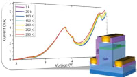
1) Ion-Conducting, Resistance Variable Memory Devices (a.k.a. memristors). These devices change resistance via the movement of metal ions (Cu and Ag ions) through an active device layer, upon proper application of an electric signal. Devices were designed that showed high speed, low voltage/current operation, variable resistance programmability (through spike-timing-dependent-plasticity tests over timing windows of ns to ms), cycling greater than 1 million cycles, and operating temperatures of at least 150°C without degradation. Many of these materials were tested in two-terminal devices, integrated with CMOS circuits, and in small cross-point arrays.
Recommendation: Based on the factors of device electrical response and ease of fabrication, the ion-conducting resistance variable memory device has the highest potential for successful application to the area of reconfigurable electronics and non-volatile memory. Based on the materials researched, this type of device also has the most flexibility in altering the device electrical characteristics to fit specific applications. Devices can exhibit bi-directional resistance tuning using low voltage, small pulse width signals. The technology can be integrated into a CMOS back-end-of-line process with no consequence to an existing CMOS fabrication facility.

2) Atomic or Molecular Memory Based on Zero-Field Splitting (ZFS). This category comprises devices that define the memory state by the interaction energy of the spin-spin and spin-orbit angular moment of the electrons around an atom and the angular momentum (spin-spin and spin-orbit) of the nucleus. The theoretical operation of this type of device is based on the energy splitting produced by this interaction (in the absence of an externally applied magnetic field), referred to as zero-field splitting. Materials were investigated to try to find a suitable material that exhibited this property at room temperature with enough electron spin density in one of the energy states for a detectable microwave signal absorption upon transition of an electron between energy states. Materials were investigated in bulk form, with some showing promise for this application, as observed via electron paramagnetic resonance spectroscopy. However, deposited thin films of these materials did not show high enough signal absorption to indicate they would be viable for detection at the nanoscale in a memory device. Preliminary device fabrication with these materials also failed to yield a functional ZFS device. This could be due to the electron density being too small in a given state to achieve a detectable signal to noise ratio.
Recommendation: The ZFS device concept is still high risk and theoretical. One approach for exploring the viability of this theory would be to investigate organic molecules as potential candidates since organic molecules frequently exhibit large spin polarization at room temperature. This increase in signal intensity due to spin polarization could give rise to a detectable signal within the small size of a bit.
Phase-Change Memory. Work in this category included devices consisting of stacked chalcogenide (S-, Se- or Te-containing material) thin films and phase-change alloys that are potentially capable of producing multiple memory states. Devices fabricated at Boise State University were large compared to the current technology node (1 um diameter vs < 20 nm). This has significant consequences for device operation due to device volume dependence (for melting and quenching the volume of material to change phase). In addition to the larger two-terminal Boise State devices, other devices fabricated on integrated circuit die with feature sizes at 0.5 um were tested. Phase-change stack materials on smaller-sized devices (40 nm) were also tested using Micron Technology’s 300 mm wafer test process flow.
Recommendation: It is difficult to change the resistance of a phase-change device consistently and between multiple values. The operation of this type of device depends significantly on the device structure and on the materials and fabrication processes. The energy required to change the resistance of a device is significantly higher than the ion-conducting memory device due to the need to heat the volume of material past the melting temperature. The device structures and fabrication processes needed in order to have lower energy switching and consistent device operation are much more complex, which translates into being more prone to processing errors. However, devices that operate with both the phase-change and an ion-conducting mechanisms within the same device material are viable.
This work was done by Kristy A. Campbell of Boise State University for the Air Force Research Laboratory. AFRL-0247
This Brief includes a Technical Support Package (TSP).
Reconfigurable Electronics and Non-Volatile Memory Research
(reference AFRL-0247) is currently available for download from the TSP library.
Don't have an account?
More From SAE Media Group
Tech Briefs
Superlattice for Sustainable Quantum Electronics

Embedded Technology INSIDER
Newly Discovered Property Could Help Keep Computer Chips Cool
Aerospace & Defense Tech Briefs
Radiation Effects on Electronics in Aligned Carbon Nanotube Technology (RadCNT)
Aerospace & Defense Tech Briefs
Fabrication and Electrical Characterization of Correlated Oxide Field Effect Switching Devices for High Speed Electronics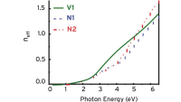
Tech Briefs
Single-Atom Transistors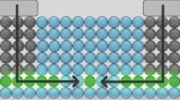
Electronics & Sensors INSIDER
Scientists Create Superconducting Semiconductor Material


Electronics & Sensors INSIDER
New Ultrathin Capacitor Could Enable Energy-Efficient Microchips
Electronics & Sensors INSIDER
Scientists Have Visualized the Electronic Structure in a Microelectronic Device
Tech Briefs
Integrating Fragile 2D Materials into Devices


Tech Briefs
Room-Temperature Magnon Switch


Tech Briefs
5 Ws of Electronic Stickers
Tech Briefs
Stable Polymeric Ink with High Conductivity
Electronics & Sensors INSIDER
Atomic Scale Semiconductor Chips — Pushing the Limits
Tech Briefs
Better Microelectronics from Coal


Tech Briefs
High-Sensitivity Microwave Radiation Sensor
Overview
The document titled "Reconfigurable Electronics and Non-Volatile Memory Research" is a final report that details the findings of a research project conducted from September 4, 2008, to October 30, 2015. The research was carried out under the auspices of the Air Force Research Laboratory (AFRL), specifically within the Space Vehicles Directorate. The report is intended for public release and aims to disseminate scientific and technical information to a broad audience, including foreign nationals.
The primary focus of the research is on reconfigurable electronics and non-volatile memory technologies. Reconfigurable electronics refer to systems that can be reprogrammed or reconfigured to perform different tasks or functions after deployment, which is particularly valuable in dynamic environments where adaptability is crucial. Non-volatile memory, on the other hand, retains data even when power is turned off, making it essential for applications where data integrity and persistence are critical.
The report outlines the methodologies employed in the research, the experimental setups, and the results obtained. It discusses the implications of these findings for future technologies, particularly in the context of space applications where reliability and performance are paramount. The research contributes to the understanding of how reconfigurable electronics can enhance system capabilities and how advancements in non-volatile memory can lead to more efficient data storage solutions.
Additionally, the document emphasizes the importance of collaboration and information exchange in advancing technological development. It highlights the role of government-funded research in fostering innovation and the necessity of making research findings accessible to the public to encourage further exploration and application of these technologies.
The report is structured to provide a comprehensive overview of the research conducted, including the significance of the findings and their potential impact on future electronic systems. It is a valuable resource for researchers, engineers, and policymakers interested in the fields of electronics and memory technology, particularly in relation to aerospace and defense applications.
In summary, this report serves as a significant contribution to the field of reconfigurable electronics and non-volatile memory, showcasing the advancements made during the research period and their relevance to future technological developments.
Top Stories
INSIDERManufacturing & Prototyping
![]() How Airbus is Using w-DED to 3D Print Larger Titanium Airplane Parts
How Airbus is Using w-DED to 3D Print Larger Titanium Airplane Parts
INSIDERManned Systems
![]() FAA to Replace Aging Network of Ground-Based Radars
FAA to Replace Aging Network of Ground-Based Radars
NewsTransportation
![]() CES 2026: Bosch is Ready to Bring AI to Your (Likely ICE-powered) Vehicle
CES 2026: Bosch is Ready to Bring AI to Your (Likely ICE-powered) Vehicle
NewsSoftware
![]() Accelerating Down the Road to Autonomy
Accelerating Down the Road to Autonomy
EditorialDesign
![]() DarkSky One Wants to Make the World a Darker Place
DarkSky One Wants to Make the World a Darker Place
INSIDERMaterials
![]() Can This Self-Healing Composite Make Airplane and Spacecraft Components Last...
Can This Self-Healing Composite Make Airplane and Spacecraft Components Last...
Webcasts
Defense
![]() How Sift's Unified Observability Platform Accelerates Drone Innovation
How Sift's Unified Observability Platform Accelerates Drone Innovation
Automotive
![]() E/E Architecture Redefined: Building Smarter, Safer, and Scalable...
E/E Architecture Redefined: Building Smarter, Safer, and Scalable...
Power
![]() Hydrogen Engines Are Heating Up for Heavy Duty
Hydrogen Engines Are Heating Up for Heavy Duty
Electronics & Computers
![]() Advantages of Smart Power Distribution Unit Design for Automotive...
Advantages of Smart Power Distribution Unit Design for Automotive...
Unmanned Systems
![]() Quiet, Please: NVH Improvement Opportunities in the Early Design...
Quiet, Please: NVH Improvement Opportunities in the Early Design...