Electro-Optic Materials Research
Developing single photon UV detection for compact chemical and biological sensors.
This report summarizes the main lines of effort for the Electro-Optics Materials Research (EOMR) program including its goals and major accomplishments, focusing on the past 5 years. This EOMR program was an effort within 601102A.31B.1 titled “Optoelectronic and Integrated Photonic Materials and Device Research” for FY16-FY19 and 611102A.AA8.1 titled “Photonic Materials and Device Research” for FY20-FY21. The focus of this EOMR for most of the program was to develop novel semiconductor optoelectronic devices to reduce the size, weight, power, and cost (SWaP-C) of chemical and biological detection and identification systems.
Specifically, the program addressed the need for high sensitivity photodetectors in the near-UV (NUV) spectrum between 300 and 350 nm for biological agent detection using light-induced fluorescence techniques employed by the Tactical Biological (TAC-BIO) detector, developed by the US Army Combat Capabilities Development Command Chemical Biological Center, as well as in the deep UV spectrum (220-240 nm) important for standoff chemical detection based upon fluorescence-free Raman spectroscopy. Late in the program, this effort pivoted to address assured communications challenges relevant to the Army modernization priority for future networks through examining how to improve the efficiency of solar-blind UV LEDs.
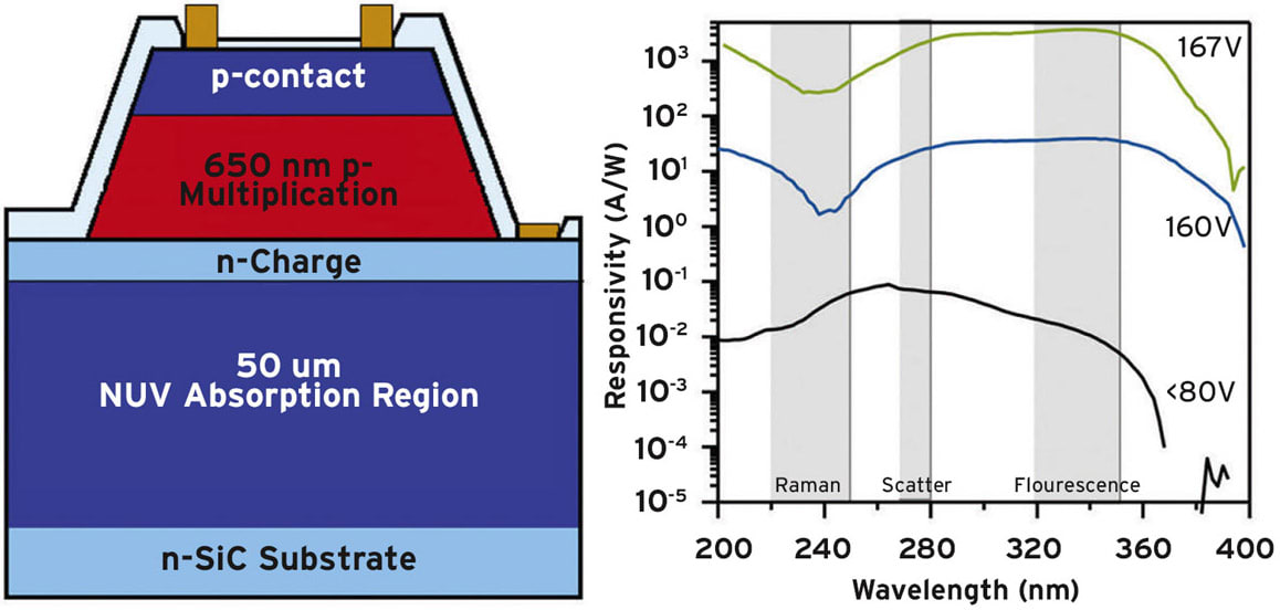
One of the four lines of effort for this work includes a focus on Near-UV Avalanche Photodiodes Based upon Silicon Carbide (NUV-SiC APDs). The goal of this effort was to demonstrate high-sensitivity APDs using SiC semiconductors that could replace commercially available photomultiplier tubes in the TAC-BIO detector so as to reduce the cost of the sensor by half as well as improve the overall ruggedness of the system. We demonstrated a separate absorption charge multiplication SiC APD with broad responsivity from 200 to 350 nm and gain greater than 106 by successfully addressing the key technical challenge of improving the collection of NUV photogenerated carriers within the device.
A second line of effort focuses on Deep-UV Avalanche Photodiodes Based upon Silicon Carbide (DUV-SiC APDs). The goal of this effort was to demonstrate high-sensitivity APDs using SiC semiconductors to replace commercially available intensified charge-coupled device (iCCD) detectors used by standoff chemical detections systems, like the PRIED (Portable Raman Improvised Explosive Detector) developed by Alakai Defense System, so as to greatly reduce SWaP-C. SiC APDs demonstrating multiplication gain greater than 5 x 10⁶ at 12 pW of 240-nm illumination and approximately 12-nA/cm2 dark current at gain of 1,000, suitable for single photon counting, were demonstrated by addressing the key technical challenge of suppressing the effects of surface recombination on the collection of DUV photogenerated carrier within the device.
A third line of effort focuses on carrier dynamics in III-Nitride semiconductor LEDs. To help design more-efficient UV devices, this effort researched the carrier dynamics in these materials through time-resolved photoluminescence (TRPL) techniques supported by modeling using a non-equilibrium Green’s function (NEGF) technique. It was shown that the fast photoluminescence (PL) lifetime (how long excited electrons exist before recombining to give off light) observed in these wide bandgap materials could be modeled by a strong excitonic recombination that dominated up to room temperature.
A fourth line of effort focused on non-polar Cubic-III-Nitride semiconductors for LEDs. The idea of this project was to study the relatively unexplored cubic aluminum gallium nitride (AlGaN) material system and investigate its doping properties and radiative emission efficiency to compare its performance against the traditional hexagonal-AlGaN material system. It was learned that heteroepitaxial growth initiation of cubic-AlGaN on the cubic silicon carbide (3C-SiC) using previous processes developed for cubic indium gallium nitride (InGaN) created too many extended defects for useful devices. This problem was attributed to the higher temperature needed for Al incorporations. Possible solutions for future efforts were outlined.
This work was performed by Gregory Garrett and Anand Sampath for the Army Research Laboratory. For more information, download the Technical Support Package (free white paper) at mobilityengineeringtech.com/tsp under the Sensors category. ARL-9477
This Brief includes a Technical Support Package (TSP).
Electro-Optic Materials Research
(reference ARL-9477) is currently available for download from the TSP library.
Don't have an account?
Overview
The Summary Technical Report on Electro-Optic Materials Research (EOMR) covers the program's efforts from October 2017 to September 2021, focusing on advancements in optoelectronic materials and devices aimed at enhancing chemical and biological detection systems. The report outlines the program's goals, major accomplishments, and the evolution of its focus over the five-year period.
Initially, the EOMR program, part of the broader "Optoelectronic and Integrated Photonic Materials and Device Research," aimed to develop novel semiconductor optoelectronic devices to improve the size, weight, power, and cost (SWaP-C) of detection systems. A significant emphasis was placed on creating high-sensitivity photodetectors for the near-UV (NUV) spectrum (300-350 nm) to facilitate biological agent detection using light-induced fluorescence techniques. This was particularly relevant for the Tactical Biological (TAC-BIO) detector developed by the US Army Combat Capabilities Development Command Chemical Biological Center. Additionally, the program addressed the need for deep UV detection (220-240 nm) for standoff chemical detection through fluorescence-free Raman spectroscopy.
One of the key lines of effort was the development of Near-UV Avalanche Photodiodes based on Silicon Carbide (NUV-SiC APDs). The goal was to create high-sensitivity APDs that could replace traditional photomultiplier tubes in the TAC-BIO detector, thereby reducing costs and enhancing system ruggedness. The report highlights the successful demonstration of a separate absorption charge multiplication SiC APD with broad responsivity from 200 to 350 nm and a gain exceeding 10^6, overcoming significant technical challenges in carrier collection.
As the program progressed, it pivoted to address assured communication challenges relevant to Army modernization, particularly in RF-congested and RF-denied environments. The report emphasizes the need for efficient UV light sources and high-sensitivity Geiger-mode UV APDs, recommending partnerships with industry to leverage expertise in device design and testing to accelerate advancements in this area.
In conclusion, the report encapsulates the EOMR program's significant contributions to the field of optoelectronic materials, highlighting its adaptability to emerging needs and its commitment to enhancing the capabilities of the Army's detection and communication systems.
Top Stories
INSIDERDefense
![]() New Raytheon and Lockheed Martin Agreements Expand Missile Defense Production
New Raytheon and Lockheed Martin Agreements Expand Missile Defense Production
NewsAutomotive
![]() Ford Announces 48-Volt Architecture for Future Electric Truck
Ford Announces 48-Volt Architecture for Future Electric Truck
INSIDERManufacturing & Prototyping
![]() Active Strake System Cuts Cruise Drag, Boosts Flight Efficiency
Active Strake System Cuts Cruise Drag, Boosts Flight Efficiency
ArticlesTransportation
![]() Accelerating Down the Road to Autonomy
Accelerating Down the Road to Autonomy
INSIDERMaterials
![]() How Airbus is Using w-DED to 3D Print Larger Titanium Airplane Parts
How Airbus is Using w-DED to 3D Print Larger Titanium Airplane Parts
Road ReadyTransportation
Webcasts
Electronics & Computers
![]() Cooling a New Generation of Aerospace and Defense Embedded...
Cooling a New Generation of Aerospace and Defense Embedded...
Power
![]() Battery Abuse Testing: Pushing to Failure
Battery Abuse Testing: Pushing to Failure
Connectivity
![]() A FREE Two-Day Event Dedicated to Connected Mobility
A FREE Two-Day Event Dedicated to Connected Mobility
Automotive
![]() Quiet, Please: NVH Improvement Opportunities in the Early Design Cycle
Quiet, Please: NVH Improvement Opportunities in the Early Design Cycle
Transportation
![]() Advantages of Smart Power Distribution Unit Design for Automotive &...
Advantages of Smart Power Distribution Unit Design for Automotive &...
Aerospace
![]() Sesame Solar's Nanogrid Tech Promises Major Gains in Drone Endurance
Sesame Solar's Nanogrid Tech Promises Major Gains in Drone Endurance

