


MEMS Wafer Inspection

Sonoscan’s AW322 200 automated system for ultrasonic inspection of MEMS wafers images and identifies internal gap-type defects down to 5 µm in size. It is especially useful for finding non-bonds, voids, and other defects in the seals surrounding the MEMS wafer cavities. System features include two loadports, two stages, and multiple transducers, enabling it to image two 8-in MEMS wafers simultaneously. Other models in the series accommodate wafer sizes of 100-300 mm. In operation, the robotic handling station counts and unloads wafers from the carriers, aligns wafers for scanning, and positions wafers on the stage. After scanning, both the acoustic wafer image and the wafer data can be used for accept/reject determination.
More From SAE Media Group

Aerospace & Defense Tech Briefs
Tips for Reducing Error When Using Eddy Current Measuring Techniques
Tech Briefs
Extrans Permeation Measurement System
Aerospace INSIDER
A New Quantum Materials Research System
Tech Briefs
SiC-Based Microstructures for Sensors
Aerospace INSIDER
3D Ultrasound Shows Aircraft Defects
Aerospace & Defense Tech Briefs
Ruggedizing Coaxial and Fiber Optic Cable Assemblies from Mechanical Strain
Aerospace & Defense Tech Briefs
Zwick Roell Provides Flexible Materials Testing over a Wide Temperature Range
Aerospace & Defense Tech Briefs
Advances in Adhesive Joining of Structural Components Focus of New Book from SAE International
Aerospace & Defense Tech Briefs
SAE International Issues First Technical Standards for Aerospace Additive Manufacturing
Aerospace & Defense Tech Briefs
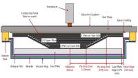
Sensing Applied Load and Damage Effects in Composites with Nondestructive Techniques
Aerospace & Defense Tech Briefs
Thermal Conductivities of Some Polymers and Composites

Tech Briefs
Product of the Month
Aerospace Manufacturing and Machining INSIDER
Supercritical Fluid Extractor
Aerospace & Defense Tech Briefs
Designing for Space and Other Extreme Environments
Aerospace INSIDER
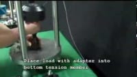
Tension/compression Load Cell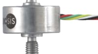
Aerospace & Defense Tech Briefs
Cold Spray Technology
Aerospace & Defense Tech Briefs
Additive Manufacturing Adoption Up, Growing Rapidly in Aerospace
Aerospace & Defense Tech Briefs
Green’s Function Extraction from Atmospheric Acoustic Propagation


Aerospace & Defense Tech Briefs
Measuring Propellant Stress Relaxation Modulus Using Dynamic Mechanical Analyzer
Aerospace & Defense Tech Briefs
3D Meta-Optics for High-Energy Lasers
Aerospace & Defense Tech Briefs
New AFRL Chamber Enhances Equipment Performance in Extreme Environments
Top Stories
INSIDERManufacturing & Prototyping
![]() How Airbus is Using w-DED to 3D Print Larger Titanium Airplane Parts
How Airbus is Using w-DED to 3D Print Larger Titanium Airplane Parts
INSIDERManned Systems
![]() FAA to Replace Aging Network of Ground-Based Radars
FAA to Replace Aging Network of Ground-Based Radars
NewsTransportation
![]() CES 2026: Bosch is Ready to Bring AI to Your (Likely ICE-powered) Vehicle
CES 2026: Bosch is Ready to Bring AI to Your (Likely ICE-powered) Vehicle
NewsSoftware
![]() Accelerating Down the Road to Autonomy
Accelerating Down the Road to Autonomy
EditorialDesign
![]() DarkSky One Wants to Make the World a Darker Place
DarkSky One Wants to Make the World a Darker Place
INSIDERMaterials
![]() Can This Self-Healing Composite Make Airplane and Spacecraft Components Last...
Can This Self-Healing Composite Make Airplane and Spacecraft Components Last...
Webcasts
Defense
![]() How Sift's Unified Observability Platform Accelerates Drone Innovation
How Sift's Unified Observability Platform Accelerates Drone Innovation
Automotive
![]() E/E Architecture Redefined: Building Smarter, Safer, and Scalable...
E/E Architecture Redefined: Building Smarter, Safer, and Scalable...
Power
![]() Hydrogen Engines Are Heating Up for Heavy Duty
Hydrogen Engines Are Heating Up for Heavy Duty
Electronics & Computers
![]() Advantages of Smart Power Distribution Unit Design for Automotive...
Advantages of Smart Power Distribution Unit Design for Automotive...
Unmanned Systems
![]() Quiet, Please: NVH Improvement Opportunities in the Early Design...
Quiet, Please: NVH Improvement Opportunities in the Early Design...