


Moving Targets: How Improvements to SiC, GaN Power Electronics Will Redefine EV
Smaller devices that can do the same or more efficient work than silicon can lead to markedly smaller EV powertrain components.

Better power electronics are on the way, thanks to private-public efforts that go back years.
This story starts in 2017, when the Department of Energy’s U.S. DRIVE partnership laid out targets for power electronics for 2025 in a technical team roadmap: power density of 100 kW/l for a powertrain that would last either 300,000 miles or 15 years, at a cost of no more than $2.70 per kW.
Progress in the intervening years led to an updated roadmap in 2024, specifying stricter 2025 targets of 150 kW/l power density at a cost of no more than $1.80 per kW, based on a 600-volt system. Along with that came more refined targets for 2030 and 2035. For 2030, the goal is an 800-volt system that produces peak power of 200 kW maintained for 30 seconds, and a power density of 200 kW/l that costs no more than $1.35 per KW. The goal for 2035 now sits at 225 kW/L for $1.20.

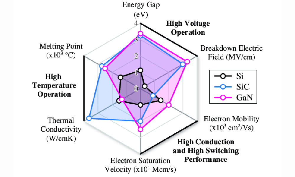
One area of focus is improving bandgap power. Bandgap is the amount of energy needed to get an electron from a valence band around the nucleus of an atom to the conduction band. Using silicon’s 1.1 electronvolt (eV) bandgap as a reference, wide bandgap generally refers to materials with a bandgap of at least 3 eV. For the purposes of power electronics, a higher bandgap is better. The U.S. DOE’s Advanced Materials and Manufacturing Technologies Office (AMMTO) put out a draft paper titled “Wide Bandgap Power Electronics Strategic Framework” in January on wide bandgap (WBG) and ultra-wide bandgap (UWBG) devices. The paper’s Executive Summary asserts, “the opportunities for design and manufacturing improvements are [so] significant that the future of the power electronics industry is mainly through leveraging WBG and UWBG materials.”
“First of all, you can get higher breakdown voltages because you need higher voltages to get that energy to move,” Burak Ozpineci, section head of the Vehicle and Mobility Systems Research Section at the Oak Ridge National Laboratory (ORNL), told SAE Media.
“You don't want the electrons moving by themselves without you triggering them.”
Wolfspeed, which supplies devices to ORNL, said that the breakdown voltages of its 1.2 kV silicon carbide (SiC) MOSFETs are several hundred volts above those for traditional silicon with the same voltage rating. Power technology company Onsemi says the breakdown field for SiC and gallium nitride (GaN) in megavolts per centimeter is ten times greater than that of Si.
Jens Baringhaus, chief expert for WBG Technologies at Bosch, highlighted a phenomenon related to bandgap. “The most important property for PE applications is not the wider bandgap but the higher critical electric field which is associated with it. A higher critical electric field allows us to design power devices which can handle the same voltages as Si devices [with] much lower resistance.”
Thanks to these and other material benefits, WBG devices are more efficient than silicon, delivering lower conduction and switching losses, along with faster switching speeds. They can handle far higher operating temperatures and power densities, and exhibit much better heat dissipation, which increases the tolerance for high ambient temperatures. The result is smaller devices that can do the same or better work than silicon, leading to markedly smaller EV powertrain components.
The two wide bandgap materials currently getting the lion’s share of attention are, as expected, SiC and GaN.
Silicon Carbide
SiC’s bandgap is about 3.3 eV. Devices are more compact than equivalent silicon devices, with excellent thermal management and high efficiency, Bosch’s Baringhaus saying that 800 volts “is a sweet spot for SiC from the cost/performance perspective.” This makes SiC good in EV applications like the traction inverter and onboard charger. ORNL’s Ozpineci said, “When we built inverters in the lab, we got over 98.5% efficiency, sometimes 99% efficiency. For silicon inverters, we would typically get around 97%.” A two-thirds reduction in losses equates to a 66% improvement.
Ozpineci said the lab’s SiC-based components also generate two-thirds less heat, too. A smaller footprint with less heat means smaller ancillaries as well, such as smaller cooling circuits with less draw. He said that when the lab built an inverter this year for the U.S. DRIVE 2025 targets, “we built an inverter that is more than eight times smaller than a similar inverter from 2015.”
These benefits accrue throughout an EV powertrain, resulting in longer EV ranges – up to 6%, according to Bosch – or, if the design is to hold range steady, lower battery costs. Multiply these benefits throughout the EV ecosystem, from chargers and motors to converters and rectifiers, and it’s clear how the benefits stack.
Gallium Nitride
At 3.4 eV, GaN’s bandgap is a whisker better than SiC. However, the first commercialized SiC device launched in 2001, the first SiC MOSFET appeared about ten years ago, leaving GaN a long way behind on the research curve. GaN devices, known as high-electron mobility transistors (HEMTs), are more efficient and compact than SiC equivalents and will eventually enable faster switching speeds, with slightly lower thermal management properties.
The material comes with a few hitches at the moment. Commercially available GaN devices are lateral devices, with the current moving horizontally across the upper portion from source through gate to drain. Silicon and SiC devices are vertical, with the current moving from source and gate at the upper surface to drain at the bottom. The lateral architecture makes the electric field management much more demanding compared to vertical devices like Si and SiC and lowers lateral GaN‘s potential voltage ratings. This makes GaN-based components best in EV applications like DC-DC converters, where higher switching frequencies are especially useful.
On top of this, among lateral GaN HEMTs, there are two types: e-GaN, which are normally off and need a positive voltage to turn on, and d-GaN, which are normally on and need a negative voltage to turn off. Automaker OEMs are said to prefer the normally-off e-GaN devices, but Baringhaus notes that, “differences between technologies at different suppliers … [have a] large impact on the performance.”
Chip makers are working on vertical GaN devices, too. One of the primary challenges is that lateral GaN devices are built on a different substrate, such as silicon or even sapphire. “If you can grow gallium nitride by itself and make it thick enough, then you can have vertical gallium nitride devices,” Ozpineci said. The issue then becomes cost.
“Vertical GaN manufactured on native GaN substrates … heavily struggles with the cost side,” Bosch’s Baringhaus said. “Reaching competitiveness against SiC will be extremely hard with native GaN substrates.” The nearer-term key is finding a substrate with an acceptable balance of cost and performance. “There are large technical hurdles for vertical GaN, and new processes need to be developed,” Baringhaus said. “Readiness for use is not expected until the end of this decade if these challenges can be mastered.”
Ozpineci, who starting working with SiC in 2001, takes a long view.
“Silicon carbide went through these things over the years, too,” he said. “In the beginning, 20 years ago, we would hear all kinds of defects that would cause issues with the devices. But they worked on those things so that they could launch them commercially.”
Challenges

SiC MOSFETS have been adopted by a growing number of automakers since 2017, and as adoption continues to grow among EV makers, the science continues to advance. Baringhaus said that in just the past year, “It became clear that SiC MOSFETs based on trench technology are not only delivering best performance but also surpass their planar gate counterparts in terms of robustness. New device concepts such as superjunction technology in SiC, which promise an additional performance boost, also profit a lot from using SiC trench technology.”
Challenges abound, though, such as miniaturization throughout the system. Maximizing the benefits of smaller devices requires optimizations such as smaller peripherals and new cooling circuits, perhaps even new liquid cooling concepts beyond water ethylene glycol (WEG). Ozpenici said, “As devices get smaller, you need to have the surface area for cooling them. Usually, the silicon devices are larger in size; in silicon carbide, they cannot make larger devices.”
This goes for components like inverters as well. “We are still looking at how we can get everything smaller and how we can integrate more components,” Ozpineci said. “For example, with silicon carbide devices on the same substrate, [or] integrating more of the sensors with them. How can we integrate multiple things to make the inverter smaller and cost less?”
Speaking of cost, that’s the counterweight to all of the issues discussed so far. SiC and GaN fabrication processes necessarily make them more expensive than silicon. The materials clawback savings when considering system-wide benefits of better performance in smaller packages with smaller and less demanding peripherals. The coming advances, as with Bosch’s fourth- and fifth-gen chips, must maintain the balance or improve the math. The company is close to putting its third-gen SiC chips into serial production, and it’s working now on fourth- and fifth-generation versions—each generation defined by performance results using a smaller device area, at a lower relative cost. “Improving performance with more complex device architectures without increasing manufacturing cost is one of the main challenges for SiC,” Baringhaus said.
One way fabricators are addressing the issue is with larger wafers packed in more devices, reducing wafer material and per-unit costs. Bosch’s Dresden plant produces 300mm Si wafers. Elsewhere, SiC is mainly produced on 150mm wafers, transitioning to 200mm; Infineon announced its first deliveries of 200mm wafers in February. GaN fabrication is mainly on 150mm and 200mm wafers, with 300mm wafers in prototype production at some companies like Infineon. For typical SiC device sizes, going from a 150mm to 200mm wafer increases the number of dies per wafer by about 1.8x, while the move from 200mm to 300mm increases yield by about 2.3x.
Even with that larger wafer size, GaN is behind the cost curve compared to SiC, but the work continues. “GaN will compete with silicon carbide, probably,” Ozpineci said. “But, you know, the cost will be an issue because silicon carbide has 20, 30 years ahead of vertical gallium nitride devices.
Another area of research is assembly technologies such as silver and copper sintering. Using these metals not only increases heat tolerance for the packaged device thanks to higher melting points, these metals reduce the prevalence of PFAs, or “forever chemicals,” in semiconductor manufacturing.
And, of course, AI has been called into service. For now, Baringhaus says, “AI is already widely in use in manufacturing process control and steering. AI is also used in power device simulation, design and layouting. We will see more and more shifting to AI-based or AI-assisted development in the future.”
Everything is moving so quickly that, as with the 2025 targets, SiC and GaN developments could achieve the U.S. DRIVE partnership’s 2030 targets before the bell tolls. As Ozpineci said, “Sometimes the progress happens exponentially. You never know.”
More From SAE Media Group
Automotive Engineering
EV Energy-Management Powers-Up
Tech Briefs
Ultra-Wide-Bandgap Power Electronics
Automotive Engineering
New 300-Mm Wafer Fab Is Key to Bosch’s Chip Future
Automotive Engineering
How 3D Printing Could Add Efficiency to EV Power Electronics
Automotive Engineering
Supercharging the Fuel Cell
Battery & Electrification Technology
EV Energy Management Powers Up
Automotive Engineering
Keeping Your Silicon Cool
Aerospace & Defense Tech Briefs
High-Temperature Silicon Carbide Power Module for Military Hybrid Electric Vehicles
Automotive Engineering
Is GaN the Future for EV Chips?
Automotive Engineering
From Emissions Tech to EV Electronics


Off-Highway Engineering
Solving the Challenges of Megawatt Chargers
Automotive Engineering
WCX 2025: Vicor’s New Power Modules Arrive with 48V
Automotive Engineering
The Push for E-Powertrain Progress

Tech Briefs
Metallization for SiC Semiconductors
Off-Highway Engineering
Thermal Management for Off-Highway Vehicles
Automotive Engineering
A Resonant Solution for Fast, Flexible EV Charging
Tech Briefs
Low-Inductance DC Power Bus
Aerospace & Defense Tech Briefs
Development of High Quality 4H-SiC Thick Epitaxy for Reliable High Power Electronics Using Halogenated Precursors
Automotive Engineering
Air- or Water-Cooling Resistors for EVs: The Case for H2O
Power Electronics INSIDER
Diamond Transistors
Off-Highway Engineering
Off-Highway Vehicle Electrification Surges Ahead
Battery & Electrification Technology
Using Silver Sintering in Traction Inverter Assembly

Aerospace & Defense Tech Briefs
Compact Power Amplifier Solution for Electronic Warfare
Power Electronics INSIDER
Improved GaN-Based Semiconductor Devices for Power Electronics

Power Electronics INSIDER
World’s First N-Channel Diamond Field-Effect Transistor
Top Stories
NewsRF & Microwave Electronics
![]() Microvision Aquires Luminar, Plans Relationship Restoration, Multi-industry Push
Microvision Aquires Luminar, Plans Relationship Restoration, Multi-industry Push
INSIDERAerospace
![]() A Next Generation Helmet System for Navy Pilots
A Next Generation Helmet System for Navy Pilots
INSIDERDesign
![]() New Raytheon and Lockheed Martin Agreements Expand Missile Defense Production
New Raytheon and Lockheed Martin Agreements Expand Missile Defense Production
INSIDERMaterials
![]() How Airbus is Using w-DED to 3D Print Larger Titanium Airplane Parts
How Airbus is Using w-DED to 3D Print Larger Titanium Airplane Parts
NewsPower
![]() Ford Announces 48-Volt Architecture for Future Electric Truck
Ford Announces 48-Volt Architecture for Future Electric Truck
ArticlesAR/AI
Webcasts
Electronics & Computers
![]() Cooling a New Generation of Aerospace and Defense Embedded...
Cooling a New Generation of Aerospace and Defense Embedded...
Automotive
![]() Battery Abuse Testing: Pushing to Failure
Battery Abuse Testing: Pushing to Failure
Power
![]() A FREE Two-Day Event Dedicated to Connected Mobility
A FREE Two-Day Event Dedicated to Connected Mobility
Unmanned Systems
![]() Quiet, Please: NVH Improvement Opportunities in the Early Design Cycle
Quiet, Please: NVH Improvement Opportunities in the Early Design Cycle
Automotive
![]() Advantages of Smart Power Distribution Unit Design for Automotive &...
Advantages of Smart Power Distribution Unit Design for Automotive &...
Energy
![]() Sesame Solar's Nanogrid Tech Promises Major Gains in Drone Endurance
Sesame Solar's Nanogrid Tech Promises Major Gains in Drone Endurance