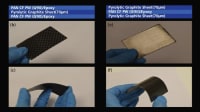
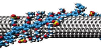
Modeling and Experimenting with 2D Materials for CMOS Type Devices and Digital Integrated Circuits
Two-dimensional transition metal dichalcogenides (2D-TMDs) have been proposed as novel optoelectronic materials for space applications due to their relatively light weight. MoS2 has been shown to have excellent semiconducting and photonic properties. Here, we report the effect of gamma irradiation on the structural and optical properties of a monolayer of MoS2.

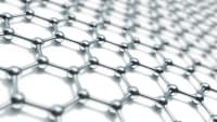
Graphene is a two-dimensional carbon material made of carbon by covalent bonds, where carbon atoms are arranged in a honeycomb lattice. Graphene has promising electronic and mechanical properties. There are many processes available for the formation of the graphene. CVD (Chemical Vapor Deposition) process for the formation of graphene over the metal surface is most compatible. Graphene is being investigated for its application in space electronics. In space, there are many irradiation particles and waves like x-rays, gamma rays, alpha particles, and beta particles. Single particle like neutron can create single event upset in electronic devices. Graphene can work as a radiation shielding material. Graphene-metal, graphene and epsilon near zero metamaterials structure can be used for electromagnetic wave absorbent.
Graphene/polymer, graphene/composite, graphene/epoxy composite material can work as an electromagnetic interface shielding material. Monolayer graphene may be used for electromagnetic interface shielding. Graphene and its derivatives can be used in biomedical applications like cancer imaging, and cancer targeting with appropriate surface engineering done on graphene. Graphene-Schottky junctions can work as low-bias radiation sensor. Since graphene is a potential material to be used in electronic devices, and radiation shielding applications, it is important to study graphene in the irradiation environment. Effects of e-beam irradiation on CVD grown graphene have been also studied.
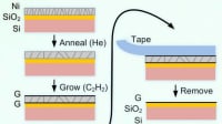
We fabricated monolayer graphene over nickel and copper substrates in Moorfield nanotechnology's nanoCVD-8G reactor by CVD process. We have investigated defects and electronic behavior of irradiated graphene by the Raman spectroscopy and X-ray photo electron spectroscopy. Most of the Raman spectroscopy studies have been done after the graphene transferred on to the SiO2/Si substrate. That process requires lift-off and other chemical processes. It can create wrinkles and defects in graphene film as well as it may increase the impurity in graphene. It creates defects at the interface which has major impact on device performance. In our studies, we deposited graphene over transition metals (Ni, Cu).
Co-60 source was used for the irradiation purpose, which has nominal irradiation dose of 207 rad/Min (±5%). We have irradiated two samples of graphene grown on nickel substrate and three samples of graphene grown on copper substrate. For the graphene grown on the nickel substrate, we exposed the irradiation dose of 100 krad (1.0 kGy) and 250 krad (2.5 kGy) on sample number one and two, respectively. On graphene grown on the copper substrate, we exposed 125 krad (1.25 kGy), 175 krad (1.75 kGy), and 265 krad (2.65 kGy) irradiation on sample number one, two, and three, respectively. These irradiation doses were used for the first set of irradiations. Raman spectroscopy and Xray photoelectron spectroscopy studies were performed on all samples (unexposed and exposed). After that, same amount of irradiation dose was subjected to samples and Raman spectroscopy and XPS studies were performed again in order to observe effect of accumulated irradiation dose.
We investigated gamma irradiation effects on a monolayer of MoS2. We studied the changes in the physical properties of MoS2 using Raman spectroscopy and XPS. The results showed that S defects dominate at lower irradiation, while Mo defects appear at higher irradiation doses. The shifting of Mo 3d and S 2p peaks in the XPS spectra confirmed the presence of S and Mo point defects. DFT studies suggest that, as the gamma irradiation dose increases, the bandgap decreases, which implies that gamma radiation-induced defects degrade the electronic conductivity of MoS2 monolayer.
This work was performed by Chintan P. Chavda and Georgios Veronis for Louisiana State University and the Air Force Research Laboratory Space Vehicles Directorate. For more information, download the Technical Support Package (free white paper) below. AFRL-20230010
This Brief includes a Technical Support Package (TSP).
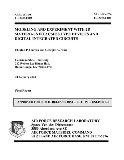
Modeling and Experimenting with 2D Materials for CMOS Type Devices and Digital Integrated Circuits
(reference AFRL-20230010) is currently available for download from the TSP library.
Don't have an account?
Overview
The document titled "Modeling and Experiment with 2D Materials for CMOS Type Devices and Digital Integrated Circuits" is a final report detailing research conducted from August 20, 2018, to August 20, 2022, under the sponsorship of the Air Force Research Laboratory. Authored by Chintan P. Chavda and Georgios Veronis from Louisiana State University, the report focuses on the application of two-dimensional (2D) materials, specifically graphene and MoS₂, in the development of complementary metal-oxide-semiconductor (CMOS) devices and digital integrated circuits.
The report is structured into several sections, beginning with a summary and introduction that outline the significance of 2D materials in modern electronics. The introduction emphasizes the potential of these materials to enhance device performance due to their unique electronic properties, which are critical for the advancement of next-generation electronic components.
The methods section details the experimental procedures employed in the research, including the growth of monolayer graphene using chemical vapor deposition (CVD) on transition metal films, and the characterization techniques utilized, such as Raman spectroscopy and X-ray photoelectron spectroscopy (XPS). The report also discusses the effects of gamma irradiation on these materials, which is explored through various experimental setups and theoretical calculations.
Results and discussion sections present findings from the Raman spectroscopy studies for both graphene and MoS₂, highlighting the impact of substrate choice on the properties of the grown monolayers. The electronic properties of MoS₂ are examined in detail, showcasing how gamma irradiation influences its characteristics. The report provides insights into the stability and performance of these 2D materials under different conditions, which is crucial for their integration into practical applications.
The conclusions summarize the key findings and their implications for future research and development in the field of electronics. The report underscores the importance of continued exploration of 2D materials for enhancing the functionality and efficiency of CMOS devices, paving the way for advancements in digital integrated circuits.
Overall, this document serves as a comprehensive resource for researchers and engineers interested in the application of 2D materials in electronics, providing valuable insights into their properties, potential applications, and the methodologies used to study them.
Top Stories
NewsRF & Microwave Electronics
![]() Microvision Aquires Luminar, Plans Relationship Restoration, Multi-industry Push
Microvision Aquires Luminar, Plans Relationship Restoration, Multi-industry Push
INSIDERAerospace
![]() A Next Generation Helmet System for Navy Pilots
A Next Generation Helmet System for Navy Pilots
INSIDERDesign
![]() New Raytheon and Lockheed Martin Agreements Expand Missile Defense Production
New Raytheon and Lockheed Martin Agreements Expand Missile Defense Production
INSIDERMaterials
![]() How Airbus is Using w-DED to 3D Print Larger Titanium Airplane Parts
How Airbus is Using w-DED to 3D Print Larger Titanium Airplane Parts
NewsPower
![]() Ford Announces 48-Volt Architecture for Future Electric Truck
Ford Announces 48-Volt Architecture for Future Electric Truck
ArticlesAR/AI
Webcasts
Electronics & Computers
![]() Cooling a New Generation of Aerospace and Defense Embedded...
Cooling a New Generation of Aerospace and Defense Embedded...
Automotive
![]() Battery Abuse Testing: Pushing to Failure
Battery Abuse Testing: Pushing to Failure
Power
![]() A FREE Two-Day Event Dedicated to Connected Mobility
A FREE Two-Day Event Dedicated to Connected Mobility
Unmanned Systems
![]() Quiet, Please: NVH Improvement Opportunities in the Early Design Cycle
Quiet, Please: NVH Improvement Opportunities in the Early Design Cycle
Automotive
![]() Advantages of Smart Power Distribution Unit Design for Automotive &...
Advantages of Smart Power Distribution Unit Design for Automotive &...
Energy
![]() Sesame Solar's Nanogrid Tech Promises Major Gains in Drone Endurance
Sesame Solar's Nanogrid Tech Promises Major Gains in Drone Endurance

