


Advances in Fabrication of Nanoscale Devices
GMR materials can be patterned to line widths of tens of nanometers.
Some advances have recently been made on several fronts in a continuing effort to develop of means of fabricating electronic and magnetic devices having dimensions of the order of tens to hundreds of nanometers. This effort is a collaboration of members, from three universities, whose interests, expertise, and facilities span synthesis of materials, nanoscale characterization, nanoscale lithography, and non-lithographic processing of nanostructures.
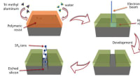
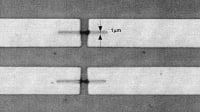
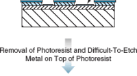
The most substantial body of work addressed the use of a novel inorganic resist material, hydrogen silsesquioxane (HSQ). This material was employed because of its potential utility as both a high-resolution resist and an etch mask. Of particular interest in this work was the use of HSQ in patterning giant-magnetoresistance (GMR) materials and their constituents (e.g., Ni, Fe, Co, and Cu). It is particularly difficult to pattern these materials at high resolution by means of dry etching because of a lack of volatile etch products. It was found that by use of either of two versions of a process involving the use of HSQ, the difficulty can be overcome sufficiently to enable the fabrication of structures in the size range of interest.
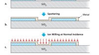
The process is summarized as follows:
- The GMR material or other material of the device that one seeks to fabricate is coated with HSQ.
- In one version of the process, the HSQ is patterned by electron-beam lithography, then etching in an argon plasma. In the other version of the process, the HSQ is patterned by use of a focused Ga+-ion beam, then etching in an argon plasma.
- The GMR or other device material exposed by the opening(s) in the patterned HSQ is removed by direct argon-ion-beam sputtering, thereby transferring the desired pattern into the device material.
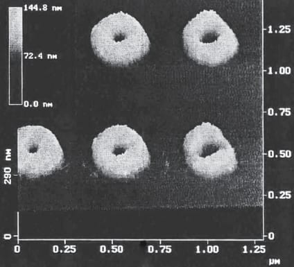
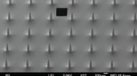
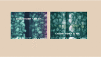
The figure shows an example of rings of a GMR material fabricated in this process. The best resolution attainable when electron- beam- lithography was used for patterning was found to characterized by a line width of about 30 nm. It was found that patterning by use of the focused Ga+ beam could be accomplished about 10 to 100 times as fast as by electron-beam lithography, but with somewhat poorer resolution characterized by a line width between 30 and 40 nm and rougher feature edges. [It should be noted that a GMR material could also be patterned directly (that is, without a resist mask) to desired shape and size by focused-ion-beam sputtering, but the GMR properties would likely be degraded.]
Another topic addressed in this work was increasing throughput in lithographic processing. One promising approach is ultra-rapid patterning of poly(methyl methacrylate) resist by sputtering induced by focused 30-keV beams of Ga+ ions.
Yet another topic addressed in this work was fabrication of semiconductor nanowires and associated structures. Advances in this area are important for the development of quantum cellular automata and other devices based on quantum dots.
This work was done by R. Hull, L. Harriott, P. Parrish; C. Chen, S. Liu, J. Graham, L. He, M. Smith of the University of Virginia; G. Snider and A. Prager of Notre Dame University; and L. Samuelson, J. Johanson, S. Nilison, and L. Montelius of Lund University for the Naval Research Laboratory.
NRL-0020
This Brief includes a Technical Support Package (TSP).
Advances in Fabrication of Nanoscale Devices
(reference NRL-0020) is currently available for download from the TSP library.
Don't have an account?
More From SAE Media Group


Tech Briefs
SiC-Based Microstructures for Sensors

Medical Design Briefs
Kirigami-Style Fabrication Enables 3D Nanostructures
Aerospace & Defense Tech Briefs
Progress Toward Carbon-Nanotube Arrays for Probing Cells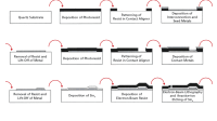
Tech Briefs
Fabricating Nanochips via Thermal Lithography
Aerospace & Defense Tech Briefs
Fabrication of Carbon Nanotube Channels on Three- Dimensional Building Blocks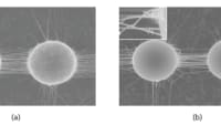

Medical Manufacturing and Machining
Atomic Blasting Creates New Devices to Measure Nanoparticles


Aerospace & Defense Tech Briefs
Fabrication of Transparent Carbon Nanotube Films for OLED Applications
Tech Briefs
Synthesizing Complex Optical Materials
Aerospace & Defense Tech Briefs
Patterning of Polycrystalline Bi2Te3 Thin Films on Silicon
Tech Briefs
Scaling Up Nano for Sustainable Manufacturing
Tech Briefs
Creating 2D All-Organic Perovskites
Tech Briefs
Kirigami-Style Fabrication at the Nanoscale
Overview
The document presents a final report on a project aimed at advancing lithographic and nanofabrication techniques for the assembly of novel nanoelectronic and nanomagnetic device structures. The project involved collaboration among researchers from the University of Virginia, Notre Dame University, and Lund University, bringing together expertise in materials synthesis, nanoscale characterization, and lithography.
The primary goal of the project was to develop new approaches to create vertical giant magnetoresistive (V-MRAM) structures, which are essential for ultra-high density magnetic random access memory. Additionally, the team explored prototype III-V semiconductor architectures for quantum cellular automata (QCA) structures. The report emphasizes the importance of three key metrics in developing new nanoscale lithographic methods: resolution, throughput, and adaptability to the device architectures being studied.
A significant focus of the research was on the application of a novel negative inorganic resist material known as hydrogen silsesquioxane (HSQ). This material was chosen for its potential as a high-resolution resist and an effective etch mask, which are critical for achieving the desired precision in nanoscale fabrication. The report details the methodologies employed in the project, highlighting the innovative techniques developed to enhance the resolution and efficiency of lithographic processes.
The document also outlines the collaborative efforts of graduate students and researchers, detailing their contributions to the project. The team’s diverse skill set and facilities allowed for a comprehensive approach to tackling the challenges associated with nanoscale device fabrication.
In summary, the report encapsulates the project's achievements in developing advanced lithographic techniques and materials for the fabrication of nanoscaled systems. It underscores the potential impact of these innovations on future technologies, particularly in the fields of memory storage and quantum computing. The findings and methodologies presented in this report contribute to the ongoing evolution of nanotechnology and its applications in various electronic devices.
Top Stories
INSIDERDefense
![]() New Raytheon and Lockheed Martin Agreements Expand Missile Defense Production
New Raytheon and Lockheed Martin Agreements Expand Missile Defense Production
NewsAutomotive
![]() Ford Announces 48-Volt Architecture for Future Electric Truck
Ford Announces 48-Volt Architecture for Future Electric Truck
INSIDERManufacturing & Prototyping
![]() Active Strake System Cuts Cruise Drag, Boosts Flight Efficiency
Active Strake System Cuts Cruise Drag, Boosts Flight Efficiency
ArticlesTransportation
![]() Accelerating Down the Road to Autonomy
Accelerating Down the Road to Autonomy
INSIDERMaterials
![]() How Airbus is Using w-DED to 3D Print Larger Titanium Airplane Parts
How Airbus is Using w-DED to 3D Print Larger Titanium Airplane Parts
Road ReadyTransportation
Webcasts
Electronics & Computers
![]() Cooling a New Generation of Aerospace and Defense Embedded...
Cooling a New Generation of Aerospace and Defense Embedded...
Power
![]() Battery Abuse Testing: Pushing to Failure
Battery Abuse Testing: Pushing to Failure
Connectivity
![]() A FREE Two-Day Event Dedicated to Connected Mobility
A FREE Two-Day Event Dedicated to Connected Mobility
Automotive
![]() Quiet, Please: NVH Improvement Opportunities in the Early Design Cycle
Quiet, Please: NVH Improvement Opportunities in the Early Design Cycle
Transportation
![]() Advantages of Smart Power Distribution Unit Design for Automotive &...
Advantages of Smart Power Distribution Unit Design for Automotive &...
Aerospace
![]() Sesame Solar's Nanogrid Tech Promises Major Gains in Drone Endurance
Sesame Solar's Nanogrid Tech Promises Major Gains in Drone Endurance