


Patterning of Polycrystalline Bi2Te3 Thin Films on Silicon
Standard photolithographic and etching recipes can be used, with suitable adaptations.
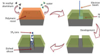
Experiments in patterning of thin films of polycrystalline bismuth telluride (Bi2Te3) on silicon substrates have been performed. Bi2Te3 is representative of a family of thermoelectric materials that are well suited for use in extracting electric energy from thermal gradients associated with flows of waste heat at temperatures in the approximate range of 0 to 150°C. Techniques and processes for fabricating macroscopic thermoelectric devices from bulk thermoelectric materials are mature and well known, but the same cannot yet be said concerning the fabrication of microscopic thermoelectric devices. The experiments reported here were performed as part of a continuing effort to develop capabilities for fabrication (including mass production) of microscopic thermoelectric devices, with a view toward eventually enabling the incorporation of them as integral parts of micro-electromechanical systems (MEMS) that could also include heat exchangers, sensors, actuators, and/or flow channels. Thus, the development of microscopic thermoelectric devices could benefit from the established industrial infrastructure for manufacturing MEMS and other silicon-based microsystems.

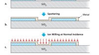
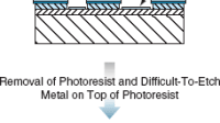
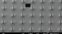
The approach followed in the experiments involved a standard procedure of (1) creating the appropriate patterns by photolithography, then (2) implementing the patterns by use, variously, of wet chemical etching or dry plasma etching to remove the Bi2Te3 from the areas outside the patterns. Established recipes for photolithography and for wet etching and dry plasma etching were used, with suitable modifications to adapt them to the materials and geometry of interest.
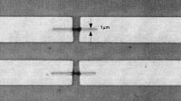
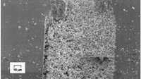
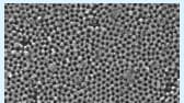
The primary adverse effect encountered in the experiments was delamination of Bi2Te3 during the development step of the photolithographic process. As shown in the figure, the Bi2Te3 adhered on and around areas containing the metal pads, but in some open areas in which the Bi2Te3 rested on bare SiO2, the Bi2Te3 was removed. It has been hypothesized that this delamination could be a result of lack of chemical bonding between the Bi2Te3 and the SiO2 surface. However, such delamination is of little concern inasmuch as in most foreseeable applications, metal pads (to which Bi2Te3 adheres, as was shown) must be included under Bi2Te3 posts to provide electrical connections.
This work was done by Brian Morgan and Patrick Taylor of the Army Research Laboratory.
ARL-0032
More From SAE Media Group

Tech Briefs
SiC-Based Microstructures for Sensors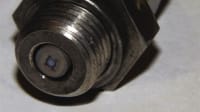


Aerospace & Defense Tech Briefs
Progress Toward Carbon-Nanotube Arrays for Probing Cells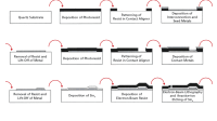
Tech Briefs
Metallization for SiC Semiconductors
Tech Briefs
A Novel Way to Convert Heat to Electricity

Tech Briefs
Fabrication of Thin-Film Type-S Thermocouples
Tech Briefs
5 Ws of Electronic Stickers
Medical Manufacturing and Machining INSIDER
New Electronics Manufacturing Process Could Lead to Breakthroughs in Prosthetics
Photonics Tech Briefs
Fabricating Small Apertures in Silicon-on-Insulator Wafers
Tech Briefs
Using 3D Printing to Strengthen Jet Engines
Medical Manufacturing and Machining
Hybrid Technique Aims to Produce Stronger, Corrosion-Resistant Nickel
Top Stories
NewsRF & Microwave Electronics
![]() Microvision Aquires Luminar, Plans Relationship Restoration, Multi-industry Push
Microvision Aquires Luminar, Plans Relationship Restoration, Multi-industry Push
INSIDERAerospace
![]() A Next Generation Helmet System for Navy Pilots
A Next Generation Helmet System for Navy Pilots
INSIDERDesign
![]() New Raytheon and Lockheed Martin Agreements Expand Missile Defense Production
New Raytheon and Lockheed Martin Agreements Expand Missile Defense Production
INSIDERMaterials
![]() How Airbus is Using w-DED to 3D Print Larger Titanium Airplane Parts
How Airbus is Using w-DED to 3D Print Larger Titanium Airplane Parts
NewsPower
![]() Ford Announces 48-Volt Architecture for Future Electric Truck
Ford Announces 48-Volt Architecture for Future Electric Truck
ArticlesAR/AI
Webcasts
Electronics & Computers
![]() Cooling a New Generation of Aerospace and Defense Embedded...
Cooling a New Generation of Aerospace and Defense Embedded...
Automotive
![]() Battery Abuse Testing: Pushing to Failure
Battery Abuse Testing: Pushing to Failure
Power
![]() A FREE Two-Day Event Dedicated to Connected Mobility
A FREE Two-Day Event Dedicated to Connected Mobility
Unmanned Systems
![]() Quiet, Please: NVH Improvement Opportunities in the Early Design Cycle
Quiet, Please: NVH Improvement Opportunities in the Early Design Cycle
Automotive
![]() Advantages of Smart Power Distribution Unit Design for Automotive &...
Advantages of Smart Power Distribution Unit Design for Automotive &...
Energy
![]() Sesame Solar's Nanogrid Tech Promises Major Gains in Drone Endurance
Sesame Solar's Nanogrid Tech Promises Major Gains in Drone Endurance