


Electronic Warfare Technology
Overcoming TWT Limitations with GaN Solid State Power Amplifiers
Military electronic warfare (EW) systems including navigation, radar guidance, terrain mapping and others, require lightweight compact components, with radio frequency (RF) output power levels to several kilowatts typically needed to meet system requirements. As GaN transistor technology advances in frequency and power output, solid state power amplifiers (SSPAs) have begun replacing traveling wave tubes (TWTs) at frequencies up to 6 GHz. The utilization of this technology results in a lower cost and greater efficiency over the life of a product.

Available TWT Technology
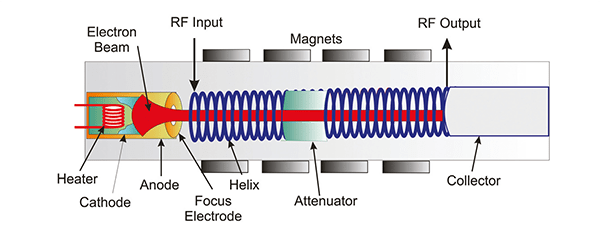
TWTs are available in two basic configurations: the cavity and the helix. Cavity TWTs are capable of very high powers— into the megawatt region—and are physically larger than helix TWTs. With their smaller size, helix TWTs lend themselves to a miniature traveling wave tube (MTWT) configuration to provide a compact, lightweight solution for UAV and other EW applications where size and weight are major issues. Yet, helix TWTs have output powers limited to approximately 2.5 kW, which is much lower than the required output for many high power applications.
While the helix TWT is operating, the heated cathode is the source for the electron beam. Electrons are accelerated toward the collector by the anode and channeled into a narrow beam by the focus electrode. An RF input signal is then applied to the helix by an input RF coupler. As the RF signal travels down the helix wire, it absorbs energy from the electron beam providing gain and increased power as the RF moves along the helix wire. The RF output is coupled off of the helix coil by the output coupler.
Decreasing Risk through SSPAs
Reliability and life of a TWT fall into three major categories:
- Infant Mortality
- Cathode Exhaustion
- Mean Time Between Failures (MTBF)
Infant Mortality
Generally an issue with all electronic hardware including solid state power amplifiers, infant mortality is controlled by amplifier burn-in at the manufacturing facility. TWTs also have an additional concern if they are stored for a long period of time. Specifically, there is the potential for damage when first turned on after an extended storage period. To minimize damage risk, an 8 to 24 hour heater burn-in is recommended before cathode voltage is applied. SSPAs eliminate the risk associated with immediate turn-on after extended storage periods.
Cathode Exhaustion
A second reliability advantage of replacing a TWT with an SSPA is eliminating cathode exhaustion. Although there are steps that can be taken to extend cathode life in a TWT, it cannot be eliminated, resulting in the system having a finite operating lifetime. However, an SSPA eliminates the cathode exhaustion issue altogether, significantly extending the system’s operating life.
MTBF
An SSPA also enhances system integrity by eliminating single point failure sources associated with older TWT technology. Since the TWT relies on energy transfer from the electron beam into the RF signal traveling along a helix wire, all components in the tube are potential single point hard failure sources.
In contrast, the replacement SSPA uses parallel combined transistors that provide a soft fail configuration. Parallel power sources in the SSPA provide the opportunity to monitor amplifier health at multiple power stages.
Increasing Performance
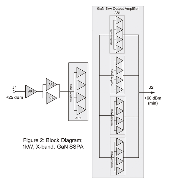
TWT amplifiers meet the output power and size requirements for compact airborne systems; however, using a TWT has some disadvantages including a finite lifetime, single point failure sources, and low reliability in harsh environments. Recent advances in GaN transistor technology have made solid state power transistors through Ku-band frequencies available. A 100 W CW GaN device at X-band is the building block for the 1 kW MTWT replacement, and the SSPA replacement has a major impact on microwave power module (MPM) reliability.
Comparative Analysis
The comparison below shows how an SSPA can operate over the 9.2 to 9.75 GHz frequency band with 1 kW peak output power at pulse widths up to 100 μsec and 10% duty cycle with an efficiency of 20%.
The X-band MPM has 60 dB of gain and operates from a 28 VDC MIL-STD- 704 airborne power bus efficiency in an 11” L X 6” W X 2” D package. Components in the MPM include a MTWT, SSPA driver, power supply and control functions.
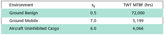
A general comparison of TWT vs. SSPA MTBF can be completed using MIL-HDBK 217. Table 1 provides the equations for calculating MTBF for a TWT based on operating environment, operating frequency and output power. The table further illustrates the MTBF results for operation at 9.5 GHz, 1 kW output power in ground benign, ground mobile and aircraft uninhibited cargo environments.
The GaN RF section of the SSPA shown in Figure 2 is a four stage design. Stages AR4 and AR5 use 0.25 μm GaN transistor technology. The design uses discrete die in multi-chip modules (MCM) for driver stage AR3 and final output stage AR4. AR4 MCMs are combined using a low loss 4-way splitter and combiner.
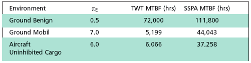
For comparison purposes, Table 2 depicts the MTBF for a 1 kW SSPA calculated using the MIL-HBDK-217 parts count method, as well as the TWT. The calculation is done at 85°C case temperature and 9.5 GHz with 10% duty cycle. The MTBF of the GaN amplifier was completed based on using ground benign, ground mobile and airborne uninhibited environments. Capacitor and resistor stresses were calculated with the SSPA case temperature at +85°C and 50% electrical stress per design guidelines and GaN transistor reliability was based on 175°C junction temperature (10% duty cycle and 85°C case temperature).
As shown in Table 2, in a passive environment like ground benign, the SSPA MTBF is about 55% greater than the TWT. However, in more challenging environments, there is a seven-fold improvement in MTBF of an SSPA compared to the TWT.
Modern Advancements
GaN technology advances including higher power density and 0.25 μm gate lengths allow GaN transistors to effectively replace TWTs at X-band.
The advantages of using a GaN SSPA to replace a TWT include:
- Eliminating a system’s finite life due to cathode exhaustion in the TWT.
- Removing concern about TWT damage at turn-on after extended storage periods.
- Eliminating multiple single point failure sources in the TWT.
- Providing distributed final stage health monitoring and early failure warning while maintaining system operational integrity.
- Offering improved reliability to meet modern EW system requirements.
As EW systems are upgraded, GaN will undoubtedly continue to advance and compete for more market share with TWTA applications due to affordability and longer system life requirements in the defense community.
This article was written by Frank Decker, Design Engineer, API Technologies (Orlando, FL). For more information, Click Here .
More From SAE Media Group
Aerospace & Defense Tech Briefs
Solid-State Microwave Power Module
Aerospace & Defense Tech Briefs
90° Hybrid Coupled Power Amplifier – Pros and Cons

Aerospace & Defense Tech Briefs
Making AESA Radar More Flexible
Aerospace & Defense Tech Briefs
Digital Radar Warning Receiver
Aerospace & Defense Tech Briefs
Compact Power Amplifier Solution for Electronic Warfare
Aerospace & Defense Tech Briefs
Broadband 1.2- and 2.4-mm Gallium Nitride (GaN) Power Amplifier Designs
Aerospace & Defense Tech Briefs
Microwave Photonic Notch Filter
Tech Briefs
Test Strategies to Track Hypersonic Threats
Aerospace & Defense Tech Briefs
RF FPGAs for Multi-Function Systems
Aerospace & Defense Tech Briefs
ONR Short Pulse Research, Evaluation and non-SWaP Demonstration for C-sUAV Study
Aerospace & Defense Tech Briefs
Radio Relays Improve Wireless Products
Aerospace & Defense Tech Briefs
Advances and Challenges in Developing Radar Applications
Aerospace & Defense Tech Briefs
Optimizing DSP Techniques for Antenna Site Software Radio
Aerospace & Defense Tech Briefs
Curled RF MEMS Switches For On-Chip Design
Aerospace & Defense Tech Briefs
Bringing RF into the Embedded World: It's Time
Aerospace & Defense Tech Briefs
Cassini Stays in Touch with NASA's Radio Science Subsystem
Aerospace & Defense Tech Briefs
How to Specify and Select RF Filters
Aerospace & Defense Tech Briefs
Unmanned Ground Vehicle Communications Relays
Aerospace & Defense Tech Briefs
Ka-Band Front-End Monolithic Microwave Integrated Circuits (MMICs) and Transmit/Receive (T/R) Modules Testing
Aerospace & Defense Tech Briefs
Validation of Ubiquitous 2D Radar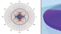
Aerospace & Defense Tech Briefs
L- and S-Band High Gain Amplifiers
Aerospace & Defense Tech Briefs
New RF Strategies for Software Radio
Aerospace & Defense Tech Briefs
Next-Generation Phased Radar Systems Lead to Hardware Improvements
Aerospace & Defense Tech Briefs
Industrial, High-Precision Joystick
Aerospace & Defense Tech Briefs
New Products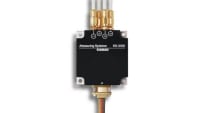
Aerospace & Defense Tech Briefs
GaN Breaks Barriers
Aerospace & Defense Tech Briefs
SIRE: A MIMO Radar for Landmine and IED Detection
Aerospace & Defense Tech Briefs
Enhance EMC Testing with Digital IF
Aerospace & Defense Tech Briefs
Counter UAV System
Top Stories
INSIDERManufacturing & Prototyping
![]() How Airbus is Using w-DED to 3D Print Larger Titanium Airplane Parts
How Airbus is Using w-DED to 3D Print Larger Titanium Airplane Parts
INSIDERManned Systems
![]() FAA to Replace Aging Network of Ground-Based Radars
FAA to Replace Aging Network of Ground-Based Radars
NewsTransportation
![]() CES 2026: Bosch is Ready to Bring AI to Your (Likely ICE-powered) Vehicle
CES 2026: Bosch is Ready to Bring AI to Your (Likely ICE-powered) Vehicle
NewsSoftware
![]() Accelerating Down the Road to Autonomy
Accelerating Down the Road to Autonomy
EditorialDesign
![]() DarkSky One Wants to Make the World a Darker Place
DarkSky One Wants to Make the World a Darker Place
INSIDERMaterials
![]() Can This Self-Healing Composite Make Airplane and Spacecraft Components Last...
Can This Self-Healing Composite Make Airplane and Spacecraft Components Last...
Webcasts
Defense
![]() How Sift's Unified Observability Platform Accelerates Drone Innovation
How Sift's Unified Observability Platform Accelerates Drone Innovation
Automotive
![]() E/E Architecture Redefined: Building Smarter, Safer, and Scalable...
E/E Architecture Redefined: Building Smarter, Safer, and Scalable...
Power
![]() Hydrogen Engines Are Heating Up for Heavy Duty
Hydrogen Engines Are Heating Up for Heavy Duty
Electronics & Computers
![]() Advantages of Smart Power Distribution Unit Design for Automotive...
Advantages of Smart Power Distribution Unit Design for Automotive...
Unmanned Systems
![]() Quiet, Please: NVH Improvement Opportunities in the Early Design...
Quiet, Please: NVH Improvement Opportunities in the Early Design...