


MEMS Resettable Circuit Breaker and Switch for DC-DC Voltage Converters
These circuit breaker cantilevers use silicon dioxide for temperature compensation.
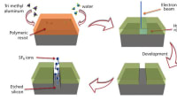
Resettable circuit breaker cantilevers use silicon dioxide (SiO2) for temper ature compensation. The compressive stress in the SiO2 causes the cantilever to bow upwards 400 μm after release. In the DC-DC voltage converter, the gap between the electrodes is 1.4 μm. After release, the cantilevers are stuck down. A short-loop experiment was conducted to better understand the cantilever behavior by omitting the contact metal and SiO2 layers from test cantilevers.
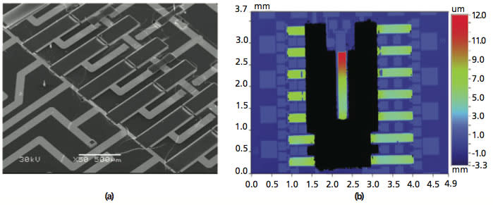
The SOI and DSP wafers were bonded together using Au-Au thermal compression bonding at 360 oC with a force of 800N for 45 minutes. Following the bonding, the handle silicon was etched using deep reactive ion etching (DRIE). To release the cantilevers, the buried oxide on the SOI wafer was etched using reactive ion etch (RIE). The figure shows a scanning electron microscope (SEM) image and an optical profilometer image of the MEMS switch for a DC-DC voltage converter. The smaller cantilevers (<1000 μm) have a slight downward bow that is due to thermal effects and permanent deformation of the metals during bonding, or a thermal and charging effect from the reactive ion etch. The larger cantilevers bow enough to cause contact with the bottom electrode. The optical profilometer data suggest that the smaller cantilevers have an acceptable gap of 2-3 μm between the cantilever and the bottom electrode. Using these data, a Rev B full wafer fabrication process was developed.
For the Rev B process, the indent is increased by 2 μm to 5 μm. For the resettable circuit breaker, tensile deposited silicon nitride is used for thermal compensation in place of compressive thermally grown SiO2. The tensile stress of the silicon nitride film causes the cantilever to bow downward or come in contact with the bottom electrode, closing the circuit for the MEMS circuit breaker. For the DC-DC voltage converter, thinner (200 nm) SiO2 is used as contact isolation material at each cantilever tip. This balances the tensile stress from metal with compressive stress from oxide, keeping the cantilever from touching the bottom electrode. The fabrication of Rev B wafers is currently in progress.
This work was done by Susana Stillwell, Sunny Kedia, Weidong Wang, Shinzo Onishi, and Scott Samson of SRI International for the Office of Naval Research. For more information, download the Technical Support Package (free white paper) at www.defensetechbriefs.com/tsp under the Electronics/Computers category. ONR-0016
This Brief includes a Technical Support Package (TSP).
MEMS Resettable Circuit Breaker and Switch for DC-DC Voltage Converters
(reference ONR-0016) is currently available for download from the TSP library.
Don't have an account?
More From SAE Media Group
Tech Briefs
SiC-Based Microstructures for Sensors


Imaging Technology
Improved Starting Materials for Back-Illuminated Imagers
Tech Briefs
5 Ws of Electronic Stickers
Medical Design Briefs
MEMS Technology Powers Sterilization Cycle Counter for Medical Applications
Aerospace & Defense Tech Briefs
Patterning of Polycrystalline Bi2Te3 Thin Films on Silicon
Electronics Tech Briefs
Improved Electron-Tunneling Magnetometer
Tech Briefs
Turning Diamond into Metal
Aerospace & Defense Tech Briefs
Fabrication and Electrical Characterization of Correlated Oxide Field Effect Switching Devices for High Speed Electronics
Tech Briefs
Metallization for SiC Semiconductors

Aerospace & Defense Tech Briefs
Future Advances in Electronic Materials and Processes - Flexible Hybrid Electronics
Aerospace & Defense Tech Briefs
Progress Toward Carbon-Nanotube Arrays for Probing Cells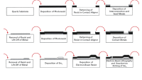
Electronics & Sensors INSIDER
MIT Engineers Grow “High-Rise” 3D Chips
Tech Briefs
Integrating Fragile 2D Materials into Devices

Electronics & Sensors INSIDER
Researchers Demonstrate a High-Speed Electrical Readout Method for Graphene Nanodevices
Electronics & Sensors INSIDER
Novel Miniaturized Organic Semiconductor Will Support Flexible Electronic Devices
Embedded Technology INSIDER
Piezoelectricity in 2D Semiconductor Holds Promise for Future MEMs
Photonics Tech Briefs
Lateral-Current-Collection HgCdTe Infrared Detectors

Tech Briefs
High-Reliability Radio Frequency MEMS Switch

Tech Briefs
Single-Atom Transistors
Electronics & Sensors INSIDER
Graphene Boosts Flexible and Wearable Electronics Boosts
Overview
The document is a Monthly Status Report for January 2010, detailing the progress of the Power MEMS Development project, specifically under contract N00014-09-C-0252, sponsored by the Office of Naval Research. Prepared by Dr. John Bumgarner, the report covers activities from January 1 to January 31, 2010.
The report highlights the development of silicon-only cantilevers and MEMS (Micro-Electro-Mechanical Systems) devices, including resettable circuit breakers and switches for DC-DC voltage converters. The fabrication process involved using silicon-on-insulator (SOI) wafers, which were patterned with release and bonding masks. The bonding of SOI and double-sided polished (DSP) wafers was achieved through Au-Au thermal compression bonding at 360ºC. Following bonding, the handle silicon was etched to allow cantilever movement, and buried oxide was removed to release the cantilevers. The report notes that smaller cantilevers exhibited a slight downward bow, potentially due to thermal effects during bonding or etching, while larger cantilevers had a more significant bow that could lead to contact with the bottom electrode.
The report also discusses the Rev B full wafer fabrication process, which included increasing the indent depth from 3.1 μm to 5 μm and replacing compressive thermally grown SiO2 with tensile deposited silicon nitride for thermal compensation. This change aimed to mitigate issues related to cantilever bowing.
In addition to cantilever development, the report outlines progress in positron trapping and storage, detailing the fabrication of MEMS-based trap structures for RF trapping of electrons. The first electron trap prototype was completed, although challenges were encountered with the surface resistance of atomic layer deposition (ALD) ZnO, which was higher than expected due to thermal gradients during deposition. Despite this, SEM analysis indicated good charge dissipation, and modifications to the deposition recipe were suggested for future iterations.
Financially, the report provides an overview of the program's budget status, indicating that current funding is sufficient for the fiscal year, with cumulative expenses reported. Overall, the document reflects significant advancements in MEMS technology development, addressing both technical challenges and financial management within the project.
Top Stories
NewsRF & Microwave Electronics
![]() Microvision Aquires Luminar, Plans Relationship Restoration, Multi-industry Push
Microvision Aquires Luminar, Plans Relationship Restoration, Multi-industry Push
INSIDERAerospace
![]() A Next Generation Helmet System for Navy Pilots
A Next Generation Helmet System for Navy Pilots
INSIDERDesign
![]() New Raytheon and Lockheed Martin Agreements Expand Missile Defense Production
New Raytheon and Lockheed Martin Agreements Expand Missile Defense Production
INSIDERMaterials
![]() How Airbus is Using w-DED to 3D Print Larger Titanium Airplane Parts
How Airbus is Using w-DED to 3D Print Larger Titanium Airplane Parts
NewsPower
![]() Ford Announces 48-Volt Architecture for Future Electric Truck
Ford Announces 48-Volt Architecture for Future Electric Truck
ArticlesAR/AI
Webcasts
Electronics & Computers
![]() Cooling a New Generation of Aerospace and Defense Embedded...
Cooling a New Generation of Aerospace and Defense Embedded...
Automotive
![]() Battery Abuse Testing: Pushing to Failure
Battery Abuse Testing: Pushing to Failure
Power
![]() A FREE Two-Day Event Dedicated to Connected Mobility
A FREE Two-Day Event Dedicated to Connected Mobility
Unmanned Systems
![]() Quiet, Please: NVH Improvement Opportunities in the Early Design Cycle
Quiet, Please: NVH Improvement Opportunities in the Early Design Cycle
Automotive
![]() Advantages of Smart Power Distribution Unit Design for Automotive &...
Advantages of Smart Power Distribution Unit Design for Automotive &...
Energy
![]() Sesame Solar's Nanogrid Tech Promises Major Gains in Drone Endurance
Sesame Solar's Nanogrid Tech Promises Major Gains in Drone Endurance