


Differential Amplifier Circuits Based on Carbon Nanotube Field Effect Transistors (CNTFETs)
Sensors, interconnects, and specialty circuits are key applications for CNT-based devices.
Since their discovery, carbon nanotubes (CNTs) have been extensively studied for their great potential in a variety of applications. Several desirable properties that CNTs possess include a high thermal conductivity, high electrical mobility, high electrical current capacity, high tensile strength, small size, compatibility with current semiconductor fabrication processes, and ability to be functionalized.
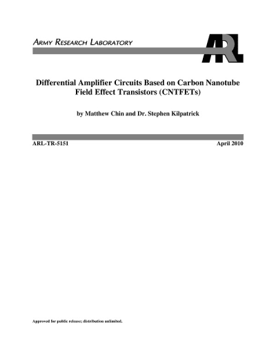
The CNT-based field effect transistor (CNTFET) was demonstrated in 1998, and has opened the door to many avenues of research. Based on the semiconducting, single-walled carbon nanotube (SWNT), CNTFETs display similar behavior to their silicon (Si) metal-oxide-semiconductor FET (MOSFET) equivalents. An oxide film is placed in between a conductive gate and the SWNTs, which acts as the channel of the transistor. Conductive metal contacts on either end of the SWNTs act as the source and drain. A bottom-gate transistor design is typically used, allowing for the SWNT channel to be exposed. This is convenient for sensor applications since the exposed CNT-based channel can be used to detect a variety of analytes via functionalization of the CNTs.
CNT-based sensors take advantage of the chemisorption of compounds onto its surface. The compounds that can be chemisorbed onto the CNT are determined by the functionalization of the CNT. In the case of a CNTFET with an exposed channel, the chemisorption of a particular compound changes the channel conductance of the CNTFET, and thus changes the source-drain current flowing through the device.
The motivation behind this research is to show proof-of-concept circuits for a CNT-based sensor that can eventually be integrated into a portable system carried by a soldier. The circuits would make use of p-channel, depletion-mode transistors built out of SWNTs with metal contacts. Such sensors could potentially be used for detecting chemical and biological agents in the field with a minimal physical and energy footprint, such as an integrated device woven into the uniform or part of an electronics package carried by the soldier.
An important first step in the research was to characterize the current CNTFET devices that the Army Research Laboratory produced in-house. This was done to gain a better understanding of the electrical characteristics and behavior of the devices. It also helped to dictate what applications they could potentially be used in as well as guide fabrication process changes that could potentially improve electrical performance in future CNTFET devices. The devices tested were back-gate, depletion-mode, p-channel FETs with undoped CNT channels and titanium (Ti)-gold (Au) source/drain metal contacts.
Measurements from 151 devices helped provide a good picture of the electrical characteristics for the CNTFETs that were produced thus far, and have provided valuable information for determining improvements that can be made to the device fabrication process. The majority of the CNTFETs currently fabricated typically behave like gate-controlled resistors, with drain-source current leakage occurring most likely due to the presence of metallic carbon nanotubes. Improvements to the fabrication process will be made in hopes of improving the performance of the CNTFETs, and pushing the electrical characteristics closer to that of a silicon-based MOSFET.
The differential amplifier is a base component in many types of active circuits, and it is the foundation for the majority of operational amplifier designs. Differential amplifiers are also used extensively in sensor applications
due to their ability to help amplify small signals and increase the signal-to-noise ratio. It is for these reasons that this research is investigating the construction of CNTFET-based differential amplifier circuits.
Initial differential amplifier measurements were made with a simplistic long-tail design. The initial experiments indicate that a change in the channel conductance is reflected in a change in the output voltage, but this change is not amplified as it typically is for silicon-based differential amplifier circuits. For every 1V difference between the two gates, the output voltage changes on the order of millivolts. Substantially more data will need to be collected and additional experiments will need to be performed to get a better picture of CNTFET-based differential amplifier circuits.
This work was done by Matthew Chin of Oregon State University and Stephen Kilpatrick of the Army Research Laboratory. For more information, download the Technical Support Package (free white paper) at www.defensetechbriefs.com/tsp under the Electronics/Computers category. ARL-0108
This Brief includes a Technical Support Package (TSP).
Differential Amplifier Circuits Based on Carbon Nanotube Field Effect Transistors (CNTFETs)
(reference ARL-0108) is currently available for download from the TSP library.
Don't have an account?
More From SAE Media Group


Aerospace & Defense Tech Briefs
Effects of Differing Carbon Nanotube Field-Effect Transistor Architectures
Tech Briefs
Fully Recyclable Printed Electronics
Tech Briefs
Silicon Carbide High-Voltage Switch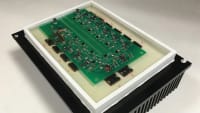

Electronics & Sensors INSIDER
Leading Experts Suggest Guidelines for Assessing Emerging Transistor Performance


Tech Briefs
Products of Tomorrow


Aerospace & Defense Tech Briefs
Magnetic Memory Devices for Embedded Computing
Tech Briefs
5Ws of the Silk Transistor

Tech Briefs
A Two-in-One Storage and Computing Device
Aerospace & Defense Tech Briefs
Procedure to Determine and Correct for Transmission Line Resistances for Direct-Current, On-Wafer Measurements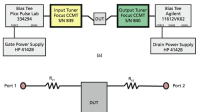
Aerospace & Defense Tech Briefs
Silicon Carbide Junction Field-Effect Transistor Devices for Scalable Solid-State Circuit Breakers
Embedded Technology INSIDER
Could Black Phosphorus be the Next Silicon?

Tech Briefs
T-Shaped Emitter Metal Structures for HBTs
Electronics & Sensors INSIDER
Tiny But Mighty: Next-Gen Transistors Hold Great Promise
Electronics & Sensors INSIDER
A New Magnetic Transistor for More Energy-Efficient Electronics
Aerospace & Defense Tech Briefs
Future Advances in Electronic Materials and Processes - Flexible Hybrid Electronics
Overview
The document titled "Differential Amplifier Circuits Based on Carbon Nanotube Field Effect Transistors (CNTFETs)" presents a progress report on research conducted from June to August 2008. Authored by Matthew Chin and Dr. Stephen Kilpatrick, it explores the application of CNTFETs in differential amplifier circuits, emphasizing their potential to improve electronic device performance.
The report begins with an introduction to CNTFETs, detailing their structure and fabrication processes. It highlights the unique properties of carbon nanotubes, which contribute to the performance characteristics of these transistors. The experimental setup and procedures used to characterize the devices are outlined, providing a foundation for the subsequent results and discussions.
Key findings from the research indicate that measurements from 151 CNTFET devices have yielded valuable insights into their electrical characteristics. The majority of the fabricated CNTFETs exhibited behavior akin to gate-controlled resistors, with issues such as drain-source current leakage attributed to the presence of metallic carbon nanotubes. This leakage poses challenges for the effective operation of the devices, suggesting areas for improvement in the fabrication process.
The report also discusses the characterization of differential amplifier circuits utilizing CNTFETs. It suggests that employing a constant current source circuit instead of a long-tail resistor could enhance the performance of these amplifiers. Initial data collected indicates promising applications for these circuits in sensor technologies, although further research is necessary to deepen the understanding of CNTFET devices and their associated circuits.
In the conclusions section, the authors summarize the progress made in understanding the electrical characteristics of CNTFETs and the implications for future device fabrication improvements. They outline the next steps for ongoing research, which include refining the fabrication techniques and exploring additional circuit configurations to optimize performance.
Overall, the document serves as a comprehensive overview of the potential of CNTFETs in differential amplifier applications, highlighting both the challenges faced and the promising avenues for future exploration. It underscores the importance of continued research in this field to unlock the full capabilities of carbon nanotube technology in electronic devices.
Top Stories
INSIDERManufacturing & Prototyping
![]() How Airbus is Using w-DED to 3D Print Larger Titanium Airplane Parts
How Airbus is Using w-DED to 3D Print Larger Titanium Airplane Parts
INSIDERManned Systems
![]() FAA to Replace Aging Network of Ground-Based Radars
FAA to Replace Aging Network of Ground-Based Radars
NewsTransportation
![]() CES 2026: Bosch is Ready to Bring AI to Your (Likely ICE-powered) Vehicle
CES 2026: Bosch is Ready to Bring AI to Your (Likely ICE-powered) Vehicle
NewsSoftware
![]() Accelerating Down the Road to Autonomy
Accelerating Down the Road to Autonomy
EditorialDesign
![]() DarkSky One Wants to Make the World a Darker Place
DarkSky One Wants to Make the World a Darker Place
INSIDERMaterials
![]() Can This Self-Healing Composite Make Airplane and Spacecraft Components Last...
Can This Self-Healing Composite Make Airplane and Spacecraft Components Last...
Webcasts
Defense
![]() How Sift's Unified Observability Platform Accelerates Drone Innovation
How Sift's Unified Observability Platform Accelerates Drone Innovation
Automotive
![]() E/E Architecture Redefined: Building Smarter, Safer, and Scalable...
E/E Architecture Redefined: Building Smarter, Safer, and Scalable...
Power
![]() Hydrogen Engines Are Heating Up for Heavy Duty
Hydrogen Engines Are Heating Up for Heavy Duty
Electronics & Computers
![]() Advantages of Smart Power Distribution Unit Design for Automotive...
Advantages of Smart Power Distribution Unit Design for Automotive...
Unmanned Systems
![]() Quiet, Please: NVH Improvement Opportunities in the Early Design...
Quiet, Please: NVH Improvement Opportunities in the Early Design...