


Effects of Differing Carbon Nanotube Field-Effect Transistor Architectures
Resulting methods can be used to produce carbon nanotube-based electronic components.
Understanding the differing methods and materials that can be used for producing carbon nanotube (CNT)- based electronic components means an informed use of materials and architectures can unleash the potential of carbon nanotube field-effect transistors (CNTFETs) for a wide array of future electronic applications.
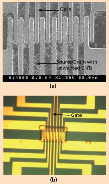
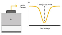
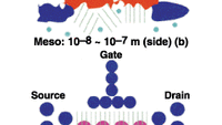
In this innovation, single-walled carbon nanotube field-effect transistors (SWCNTFETs) were fabricated with varying device architectures. Variations on the standard back-gated architecture included varying the gate oxide material and thickness, changing source and drain contact metallization, suspending the carbon nanotubes to minimize interaction with the gate oxide, and fabricating a top-gated architecture employing a thin layer of aluminum oxide (Al2O3) as the gate oxide. Devices were characterized and compared to each other based on the CNTFET properties of noise, hysteresis, sub-threshold slope, and threshold voltage. Results show that some properties of the CNTFET, such as hysteresis and noise, can be modified; other properties, however, are intrinsic to the CNT.
Annealing and the choice of gate dielectric were found to affect the device noise and the SNR. Hysteresis was shown to be a property of the CNTFET that can be, for the most part, eliminated with appropriate device geometry, such as a top-gate architecture that provides environmental passivation. This will be advantageous for electronic applications, while greater hysteresis, due to environmental exposure, may indicate a device architecture that is well suited to chemical sensing applications. While a single device architecture will not be optimum for all applications, there are a number of variables that can be tuned to optimize these devices for a given application.
This work was done by Andrew M. Dorsey and Matthew H. Ervin of the Army Research Laboratory. For more information, download the Technical Support Package (free white paper) at www.defensetechbriefs.com/tsp under the Electronics/Computers cate gory. ARL-0090
This Brief includes a Technical Support Package (TSP).
Effects of Differing Carbon Nanotube Field-Effect Transistor Architectures
(reference ARL-0090) is currently available for download from the TSP library.
Don't have an account?
More From SAE Media Group
Electronics & Sensors INSIDER
Leading Experts Suggest Guidelines for Assessing Emerging Transistor Performance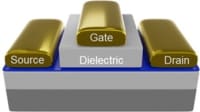
Aerospace & Defense Tech Briefs
Radiation Effects on Electronics in Aligned Carbon Nanotube Technology (RadCNT)


Tech Briefs
Polymer-Based Electrical Insulation for Circuits
Embedded Technology INSIDER
Could Black Phosphorus be the Next Silicon?
Embedded Technology INSIDER
Newly Discovered Property Could Help Keep Computer Chips Cool
Tech Briefs
Better Microelectronics from Coal
Tech Briefs
Fully Recyclable Printed Electronics


Tech Briefs
Solid-State Thermal Transistor

Electronics & Sensors INSIDER
MIT Team Takes a Major Step Toward Fully 3D-Printed Active Electronics

Aerospace & Defense Tech Briefs
Energy-Filtered Tunnel Transistor: A New Device Concept Toward Extremely Low Energy Consumption Electronics
Tech Briefs
Electronics Withstand Extreme Heat

Tech Briefs
Products of Tomorrow


Tech Briefs
Light-Emitting Tattoo


Tech Briefs
Ultrathin Transistors for Faster Computer Chips
Overview
The document titled "Effects of Differing Carbon Nanotube Field-effect Transistor Architectures" by Andrew M. Dorsey and Matthew H. Ervin, published in July 2009, investigates the performance characteristics of carbon nanotube field-effect transistors (CNT-FETs) based on varying architectural designs. The research is part of ongoing efforts to leverage the unique properties of carbon nanotubes in electronic applications, particularly in the development of high-performance transistors.
The report begins by outlining the significance of CNTs in the field of nanotechnology and electronics, highlighting their exceptional electrical, thermal, and mechanical properties. These attributes make CNTs promising candidates for next-generation semiconductor devices. The authors focus on how different architectural configurations of CNT-FETs can influence their electrical performance, including parameters such as on/off current ratios, subthreshold swing, and overall device stability.
The study employs a combination of experimental and theoretical approaches to analyze various CNT-FET designs. Key architectures examined include single-walled carbon nanotube (SWCNT) transistors and multi-walled carbon nanotube (MWCNT) transistors, each presenting distinct advantages and challenges. The authors utilize scanning electron microscopy (SEM) to provide visual evidence of the structures and to assess the quality and alignment of the nanotubes within the devices.
Results indicate that the architecture of the CNT-FET significantly impacts its electrical characteristics. For instance, the alignment and density of the nanotubes play crucial roles in determining the device's conductivity and switching speed. The report also discusses the implications of these findings for future research and development, suggesting that optimizing CNT-FET architectures could lead to substantial improvements in performance metrics.
In addition to the technical findings, the document emphasizes the importance of continued exploration in this field, as advancements in CNT technology could pave the way for more efficient and powerful electronic devices. The authors conclude by advocating for further studies to refine CNT-FET designs and to explore their integration into larger electronic systems.
Overall, this report contributes valuable insights into the design and optimization of carbon nanotube-based transistors, underscoring their potential to revolutionize the electronics industry through enhanced performance and miniaturization.
Top Stories
INSIDERManufacturing & Prototyping
![]() How Airbus is Using w-DED to 3D Print Larger Titanium Airplane Parts
How Airbus is Using w-DED to 3D Print Larger Titanium Airplane Parts
INSIDERManned Systems
![]() FAA to Replace Aging Network of Ground-Based Radars
FAA to Replace Aging Network of Ground-Based Radars
NewsTransportation
![]() CES 2026: Bosch is Ready to Bring AI to Your (Likely ICE-powered) Vehicle
CES 2026: Bosch is Ready to Bring AI to Your (Likely ICE-powered) Vehicle
NewsSoftware
![]() Accelerating Down the Road to Autonomy
Accelerating Down the Road to Autonomy
EditorialDesign
![]() DarkSky One Wants to Make the World a Darker Place
DarkSky One Wants to Make the World a Darker Place
INSIDERMaterials
![]() Can This Self-Healing Composite Make Airplane and Spacecraft Components Last...
Can This Self-Healing Composite Make Airplane and Spacecraft Components Last...
Webcasts
Defense
![]() How Sift's Unified Observability Platform Accelerates Drone Innovation
How Sift's Unified Observability Platform Accelerates Drone Innovation
Automotive
![]() E/E Architecture Redefined: Building Smarter, Safer, and Scalable...
E/E Architecture Redefined: Building Smarter, Safer, and Scalable...
Power
![]() Hydrogen Engines Are Heating Up for Heavy Duty
Hydrogen Engines Are Heating Up for Heavy Duty
Electronics & Computers
![]() Advantages of Smart Power Distribution Unit Design for Automotive...
Advantages of Smart Power Distribution Unit Design for Automotive...
Unmanned Systems
![]() Quiet, Please: NVH Improvement Opportunities in the Early Design...
Quiet, Please: NVH Improvement Opportunities in the Early Design...