


Channel Field Effect Transistors
Direct wafer bonding creates ideal channels made of extremely mismatched materials for field effect transistors.
Narrow bandgap semiconductors offer high carrier mobilities and low contact resistances, while wide bandgap semiconductors offer high breakdown voltages. A series of heterojunction transistors has been investigated and proved to be effective for improving both speed and power output. These devices include double heterostructure InP/InGaAs/InP bipolar transistors and composite-channel InAlAs/InGaAs/lnP/InAlAs high-electron-mobility transistors (HEMTs), which have taken full advantage of the matched lattice constant (or pseudomorphic growth).
However, for the most popular wide bandgap semiconductor GaN and SiC, the lattice mismatch between GaN and semiconductors with a reasonably small bandgap (including InGaN) is so large that pseudomorphic growth is very difficult. For instance, the critical thickness of InN on GaN is about one monolayer. To marry the advantages offered by both narrow bandgap and wide bandgap semiconductors, direct wafer bonding was explored for ideal channels made of extremely mismatched materials for field effect transistors.
GaAs was integrated with GaN using wafer fusion, also called direct wafer bonding. GaAs was chosen over InGaAs or InSb because it is binary and easy to obtain. The stable phase for GaAs is a zinc blend. The wafer fusion experiments not only successfully demonstrated dislocation-free integration of extremely lattice-mismatched GaAs and GaN, but also showed the improvement in breakdown voltage by employing a wide bandgap material.
This investigation demonstrated it is feasible to fabricate composite channel transistors; however, more experiments are necessary to understand the effects of the interface between the mismatched materials.
This work was done by Huili (Grace) Xing of the University of Notre Dame for the Office of Naval Research. For more information, download the Technical Support Package (free white paper) at www.defensetechbriefs.com/tsp under the Electronics/Computers category. ONR-0019
This Brief includes a Technical Support Package (TSP).

Channel Field Effect Transistors
(reference ONR-0019) is currently available for download from the TSP library.
Don't have an account?
More From SAE Media Group
Tech Briefs
Ultra-Wide-Bandgap Power Electronics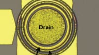


Tech Briefs
T-Shaped Emitter Metal Structures for HBTs
Aerospace & Defense Tech Briefs
Silicon Carbide Junction Field-Effect Transistor Devices for Scalable Solid-State Circuit Breakers
Tech Briefs
Silicon Carbide High-Voltage Switch
Sensor Technology
The Role of Compound Semiconductors in the IoT
Aerospace & Defense Tech Briefs
Procedure to Determine and Correct for Transmission Line Resistances for Direct-Current, On-Wafer Measurements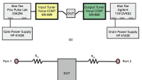
Tech Briefs
Silicon Carbide npnp Thyristors


Tech Briefs
Monolithic GaAs FET Power Amplifiers for Kₐ Band


Electronics & Sensors INSIDER
Convert Power Faster and More Efficiently
Embedded Technology INSIDER
Could Black Phosphorus be the Next Silicon?
Tech Briefs
Enhanced Material Stable Enough for Solar Cells

Electronics & Sensors INSIDER
MIT Engineers Grow “High-Rise” 3D Chips
Overview
The document is a final technical report on Ideal Channel Field Effect Transistors (FETs) prepared for the Office of Naval Research by Huili (Grace) Xing from the University of Notre Dame. It covers research conducted from July 24, 2007, to March 31, 2009, focusing on the integration of narrow and wide bandgap semiconductors to enhance the performance of electronic devices.
The report highlights the advantages of narrow bandgap semiconductors, such as high carrier mobilities and low contact resistances, alongside the benefits of wide bandgap semiconductors, which include high breakdown voltages. The research specifically addresses the challenges posed by lattice mismatches between materials, particularly between GaN (gallium nitride) and narrow bandgap semiconductors like InGaN (indium gallium nitride). The significant lattice mismatch complicates the pseudomorphic growth of these materials, which is essential for optimal device performance.
To overcome these challenges, the report explores the technique of direct wafer bonding, also known as wafer fusion. This method allows for the integration of extremely mismatched materials, enabling the fabrication of composite channel transistors. The report details the experimental formation of lattice-mismatched heterostructures, specifically GaAs (gallium arsenide) bonded to GaN. The wafer fusion process involves cleaning the surfaces of the wafers, removing native oxides, and applying pressure and heat to achieve a strong bond while maintaining the crystallinity of the materials.
The findings indicate that the integration of GaAs with GaN through wafer fusion results in dislocation-free structures, which is crucial for improving device performance. The report also discusses the electrical characteristics of the fabricated diodes, noting improvements in breakdown voltage when using GaN compared to traditional GaAs homojunctions. The measured breakdown voltage of GaAs/GaN heterostructures was found to be lower than theoretical predictions, attributed to interface defects.
Overall, the report emphasizes the feasibility of using direct wafer bonding to create high-performance transistors from mismatched semiconductor materials, paving the way for advancements in electronic devices that leverage the strengths of both narrow and wide bandgap semiconductors. Further experiments are suggested to better understand the effects of the interface between these mismatched materials.
Top Stories
INSIDERManufacturing & Prototyping
![]() How Airbus is Using w-DED to 3D Print Larger Titanium Airplane Parts
How Airbus is Using w-DED to 3D Print Larger Titanium Airplane Parts
NewsAutomotive
![]() Microvision Aquires Luminar, Plans Relationship Restoration, Multi-industry Push
Microvision Aquires Luminar, Plans Relationship Restoration, Multi-industry Push
INSIDERAerospace
![]() A Next Generation Helmet System for Navy Pilots
A Next Generation Helmet System for Navy Pilots
INSIDERDesign
![]() New Raytheon and Lockheed Martin Agreements Expand Missile Defense Production
New Raytheon and Lockheed Martin Agreements Expand Missile Defense Production
ArticlesAR/AI
![]() CES 2026: Bosch is Ready to Bring AI to Your (Likely ICE-powered) Vehicle
CES 2026: Bosch is Ready to Bring AI to Your (Likely ICE-powered) Vehicle
Road ReadyDesign
Webcasts
Semiconductors & ICs
![]() Advantages of Smart Power Distribution Unit Design for Automotive...
Advantages of Smart Power Distribution Unit Design for Automotive...
Unmanned Systems
![]() Quiet, Please: NVH Improvement Opportunities in the Early Design...
Quiet, Please: NVH Improvement Opportunities in the Early Design...
Electronics & Computers
![]() Cooling a New Generation of Aerospace and Defense Embedded...
Cooling a New Generation of Aerospace and Defense Embedded...
Power
![]() Battery Abuse Testing: Pushing to Failure
Battery Abuse Testing: Pushing to Failure
AR/AI
![]() A FREE Two-Day Event Dedicated to Connected Mobility
A FREE Two-Day Event Dedicated to Connected Mobility