


Development of GaN-Based Nanostructure Photon Emitters
The unique properties of GaN make it suitable for single-photon emitters, LEDs, VCSELs, and quantum cascade lasers.
Gallium nitride (GaN)-based wide bandgap semiconductors are very important material systems for fabrication of photon emitters in a wide range of wavelengths. In particular, the light emitters in ultraviolet (UV), blue, and green wavelengths have been developed and demonstrated in recent years. Besides these UV and visible light emitters, the unique properties of a GaN material system such as large exciton energy and large LO phonon energy, have been proposed as a very suitable material candidate for realization of various photon emitters such as single-photon emitters, LEDs, vertical cavity surface emitting lasers (VCSELs), and quantum cascade lasers (QCL) at room temperature.
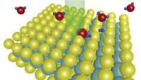
GaN-based quantum confined structures and nanostructures for control of photon emission have been developed, as well as various blue and UV emitters including the high-efficiency blue LEDs and blue VCSELs. In addition, a GaN-based quantum cascade device has been developed for generation of THz emission. All of these GaN-based photon-emitting devices are mostly grown on a foreign substrate such as sapphire, which has large lattice mismatched with GaN. As a result, there are defects in the grown nanostructures such as multiple quantum-well (MQW) structure for devices such as QCLs, LEDs, and VCSELs when the structures are grown by conventional MOCVD epitaxial growth method.
This work resulted in the development of a new epitaxial growth approach to reduce the defect density, improve epi-layer quality, and achieve better thickness control by using atomic layer deposition technique to grow MQW and various nanostructures for application in QCLs, LEDs, and VCSELs.
A viable new epitaxial growth technique was established with better thickness control, low defect density, and high-quality epitaxial film for use in growth of photonic emitters. The precision control of epitaxial layer thickness and composition are critical to GaN-based photon-emitter device performance. The understanding of the optical characteristics and structural properties of the grown structures is important for refinement and optimization of device design and growth techniques for fabrication of functional photon-emitting devices.
This work was done by Shing-Chung Wang of National Chiao Tung University for the Asian Office of Aerospace Research and Development. For more information, download the Technical Support Package (free white paper) at www.defensetechbriefs.com/tsp under the Photonics category. AFRL-0152
This Brief includes a Technical Support Package (TSP).
Development of GaN-Based Nanostructure Photon Emitters
(reference AFRL-0152) is currently available for download from the TSP library.
Don't have an account?
More From SAE Media Group
Photonics Tech Briefs
DFM Your Device? Simulation Is the Answer
Aerospace & Defense Tech Briefs
BC VCSELs for RF/Photonic Links
Aerospace & Defense Tech Briefs
On the Pulsed Laser Ablation of Metals and Semiconductors
Photonics & Imaging Technology
Using Magnets to Toggle Nanolasers Leads to Better Photonics
Photonics & Imaging Technology
Ultrafast Beam-Steering Breakthrough at Sandia Labs
Air Force Research Laboratory Technology Horizons
Patterned Gallium Arsenide Devices for Infrared Countermeasures
Photonics & Imaging Technology
Continuous and Stable Lasing Achieved From Low-Cost Perovskites at Room Temperature
Photonics & Imaging Technology
2.2-Micron, Uncooled, InGaAs Photodiodes and Balanced Photoreceivers up to 25-GHz Bandwidth
Tech Briefs
Nanoscale LED Also Functions as a Laser
Photonics & Imaging Technology
A First-Of-Its-Kind Integrated Optical Isolator
Photonics Tech Briefs
Nanotechnology’s Role in Mid-Infrared Laser Development
Photonics & Imaging Technology
A Laser That Could Reshape the Landscape of Integrated Photonics
Tech Briefs
Material Increases Efficiency of LED Devices
Photonics & Imaging Technology
How to Innovate and Overcome the Challenges of Blue Laser Beam Shaping
Photonics & Imaging Technology INSIDER
Paving the Way to Electrically Pumped Lasers from Colloidal-Quantum-Dots
Photonics & Imaging Technology
Pratt & Whitney, Virginia Tech Pioneer Laser-Optical Approach for Turbofan Engine Thrust Measurement
Photonics Tech Briefs
Multicolor Transceiver for Optoelectronic Communication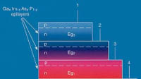
Aerospace & Defense Tech Briefs
Frequency Agile Plasmonic Antennas and Sensors

Photonics Tech Briefs
Semiconductor Quantum Dots as Radiation-Hard Light Emitters
Aerospace & Defense Tech Briefs
3D Meta-Optics for High-Energy Lasers

Photonics & Imaging Technology
Essential Principles for Designing and Specifying Laser Optics
Aerospace & Defense Tech Briefs
Fast Liquid-Crystal-on-Silicon Spatial Light Modulators
Photonics & Imaging Technology
Novel Light-Field Sensor for 3D Scene Construction Has Unprecedented Angular Resolution
Aerospace & Defense Tech Briefs
Covert Infrared Battlefield Combat Taggants
Photonics & Imaging Technology
Ultrafast Laser Micromachining
Tech Briefs
High-Power, Portable Terahertz Laser
Tech Briefs
Low-Energy Nanolaser Shines in all Directions
Overview
The document is a final report on the research project titled "Development of GaN-Based Nanostructure Photon Emitters," conducted by a research group at the National Chiao Tung University (NCTU) from July 1, 2008, to July 31, 2009. The project was supported by the National Nano Science and Technology Program Office of the National Science Council (NSC) and aimed to advance the development of gallium nitride (GaN)-based quantum confined structures and nanostructures for photon emission control.
The report highlights the significance of GaN-based wide bandgap semiconductors in fabricating photon emitters across a wide range of wavelengths, particularly in the ultraviolet (UV), blue, and green spectra. The research group successfully developed high-efficiency blue light-emitting diodes (LEDs) and blue vertical cavity surface emitting lasers (VCSELs). Additionally, they explored GaN-based quantum cascade devices for generating terahertz (THz) emissions, collaborating with experts from the U.S. Air Force Office of Scientific Research (AFOSR) and other institutions.
A major challenge faced in the growth of GaN-based devices is the use of foreign substrates, such as sapphire, which leads to significant lattice mismatches and defects in the resulting nanostructures. The report discusses the limitations of conventional metal-organic chemical vapor deposition (MOCVD) methods, which often result in high defect densities in multiple quantum well (MQW) structures used in devices like QCLs, LEDs, and VCSELs.
To address these issues, the research aimed to develop a new epitaxial growth technique using atomic layer deposition (ALD). This method allows for better control over layer thickness, reduced defect density, and improved quality of epitaxial films. The report outlines the scientific objectives, which include establishing a viable epitaxial growth technique and characterizing the optical and structural properties of the grown MQW active layer structures to verify improved device performance.
The document also references a publication resulting from this research, which discusses the high-quality ultraviolet AlGaN/GaN multiple quantum wells grown using the ALD technique. Overall, the report emphasizes the potential of GaN-based materials for various photon-emitting applications and the importance of refining growth techniques to enhance device performance.
Top Stories
INSIDERManufacturing & Prototyping
![]() How Airbus is Using w-DED to 3D Print Larger Titanium Airplane Parts
How Airbus is Using w-DED to 3D Print Larger Titanium Airplane Parts
INSIDERManned Systems
![]() FAA to Replace Aging Network of Ground-Based Radars
FAA to Replace Aging Network of Ground-Based Radars
NewsTransportation
![]() CES 2026: Bosch is Ready to Bring AI to Your (Likely ICE-powered) Vehicle
CES 2026: Bosch is Ready to Bring AI to Your (Likely ICE-powered) Vehicle
NewsSoftware
![]() Accelerating Down the Road to Autonomy
Accelerating Down the Road to Autonomy
EditorialDesign
![]() DarkSky One Wants to Make the World a Darker Place
DarkSky One Wants to Make the World a Darker Place
INSIDERMaterials
![]() Can This Self-Healing Composite Make Airplane and Spacecraft Components Last...
Can This Self-Healing Composite Make Airplane and Spacecraft Components Last...
Webcasts
Defense
![]() How Sift's Unified Observability Platform Accelerates Drone Innovation
How Sift's Unified Observability Platform Accelerates Drone Innovation
Automotive
![]() E/E Architecture Redefined: Building Smarter, Safer, and Scalable...
E/E Architecture Redefined: Building Smarter, Safer, and Scalable...
Power
![]() Hydrogen Engines Are Heating Up for Heavy Duty
Hydrogen Engines Are Heating Up for Heavy Duty
Electronics & Computers
![]() Advantages of Smart Power Distribution Unit Design for Automotive...
Advantages of Smart Power Distribution Unit Design for Automotive...
Unmanned Systems
![]() Quiet, Please: NVH Improvement Opportunities in the Early Design...
Quiet, Please: NVH Improvement Opportunities in the Early Design...