


Dynamics of Epitaxy on Nano-Sized Semiconductor Surfaces
New device applications are based on self-assembly quantum dot formation on the pre-patterned semiconductor substrates.
Semiconductor self-assembled quantum dots (QDs) have emerged as one of the simplest subjects for exploring and exploiting the physics and device applications of charge carriers and excitons in the three-dimensional confinement regime. Nanoscale-sized surfaces in the form of mesas or ridges on patterned substrates offer opportunities, not only for creating large densities of QDs with great homogeneity, but also for novel thin-film growth-control phenomena during the formation of QDs on the surfaces of Si stripe and mesa structures. Si mesa structures have been demonstrated to be an excellent template for studying homoepitaxy and heteroepitaxy phenomena.
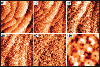
The top terraces and the side walls of silicon have very different atomic structures and dangling bond densities. During CVD, the sticking coefficients of source molecules on the two kinds of surfaces are often quite different. Also, adatoms migrate at different rates on the two surfaces. If heteroepitaxy is involved, the two interfaces will exhibit different strain fields, also, owing to different surface reconstruction. All of these factors lead to different film deposition rates and QD formation density on the top terraces and sidewalls.
Many promising new device applications are based on self-assembly QD formation on the pre-patterned semiconductor substrates. Numerous groups are currently working on better control of QDs’ density, size homogeneity, and position ordering, yet the detailed, atomic-resolved, and in situ observation of the self-assembly growth is still lacking. This proposed research intends to fabricate patterned stripe and mesa structures with well-defined sidewalls. With the help of variable-temperature SPM on the patterned substrates, the atomistic CVD growth mechanism of QDs on the top terraces as well as on the sidewalls are to reveal the structure evolution of all surface areas on a substrate, and the very initial stage of QDs’ formation.
This work was done by Deng-Sung Lin of the Institute of Physics, Taiwan, for the Air Force Research Laboratory. AFRL-0127
This Brief includes a Technical Support Package (TSP).
Dynamics of Epitaxy on the Nano-sized Semiconductor Surfaces
(reference AFRL-0127) is currently available for download from the TSP library.
Don't have an account?
More From SAE Media Group
Electronics & Sensors INSIDER
Researchers Create First Functional Semiconductor Made from Graphene
Electronics & Sensors INSIDER
Scientists Create Superconducting Semiconductor Material
Electronics & Sensors INSIDER
Researchers Wire Up Individual Graphene Nanoribbons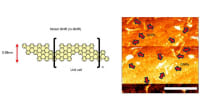
Aerospace & Defense Tech Briefs
Gallium Nitride High-Power Electronics
Aerospace & Defense Tech Briefs
Development of High Quality 4H-SiC Thick Epitaxy for Reliable High Power Electronics Using Halogenated Precursors
Tech Briefs
Turning Diamond into Metal
Tech Briefs
Single-Atom Transistors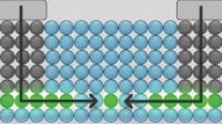
Electronics & Sensors INSIDER
2D Materials for Extra Thin Computer Chips
Electronics & Sensors INSIDER
Graphene-Based Electronics

Imaging Technology
Improved Starting Materials for Back-Illuminated Imagers


Photonics & Imaging Technology
Measuring Surface Roughness with an Atomic Force Microscope
Tech Briefs
Transparent Graphene Electrodes


Tech Briefs
Fluoride Materials for Extra-Thin Computer Chips
Photonics & Imaging Technology
Individual Quantum Dots Imaged in 3-D for the First Time

Electronics & Sensors INSIDER
Graphene Boosts Flexible and Wearable Electronics Boosts
Embedded Computing INSIDER
2D Electronic Devices Could Replace Silicon
Aerospace & Defense Tech Briefs
MEMS Resettable Circuit Breaker and Switch for DC-DC Voltage Converters
Embedded Technology INSIDER
“Tuning” Graphene Drums Might Turn Conductors Into Semiconductors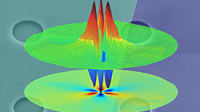

Overview
The document titled "Dynamics of Epitaxy on the Nano-sized Semiconductor Surfaces" is a final technical report authored by Deng-Sung Lin, covering research conducted from March 14, 2005, to September 8, 2006. The report focuses on the study of semiconductor self-assembled quantum dots (QDs), which are nanoscale structures that exhibit unique electronic and photonic properties due to their size-dependent energy levels.
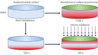
The primary objective of the research is to gain a fundamental understanding of the crystal growth phenomena associated with QDs on patterned semiconductor surfaces, specifically silicon (Si) substrates. The study emphasizes the importance of creating well-defined patterned structures, such as mesas and stripes, with flat (111) sidewalls. This is achieved through lithography and anisotropic wet chemical etching techniques. The report highlights the use of variable-temperature scanning probe microscopy (VT-SPM) to observe the chemical vapor deposition (CVD) growth mechanisms of QDs in real-time, both on the top terraces and sidewalls of these pre-patterned structures.
The document outlines the significance of QDs in semiconductor physics, noting their potential applications in optoelectronic devices due to their high optical efficiency. The research aims to improve the long-range spatial ordering of QDs, which is crucial for enhancing device performance. By selectively growing QDs on finite-sized surfaces, the study seeks to control their position, lateral coupling, and density, which are essential for the development of advanced electronic and optoelectronic applications.
Additionally, the report discusses the differences in epitaxial growth behavior on nanoscale surfaces compared to traditional surfaces, indicating that the unique characteristics of these small structures can lead to more predictable and tunable growth outcomes. The findings from this research are expected to provide valuable insights for researchers working on QD fabrication and contribute to the advancement of device applications in the field of nanotechnology.
The document concludes with a budget section, detailing the financial aspects of the research project, and includes references to previous studies that have laid the groundwork for this investigation. Overall, the report presents a comprehensive overview of the dynamics of epitaxy on nanoscale semiconductor surfaces, emphasizing its relevance to the future of semiconductor technology.
Top Stories
INSIDERManufacturing & Prototyping
![]() How Airbus is Using w-DED to 3D Print Larger Titanium Airplane Parts
How Airbus is Using w-DED to 3D Print Larger Titanium Airplane Parts
INSIDERManned Systems
![]() FAA to Replace Aging Network of Ground-Based Radars
FAA to Replace Aging Network of Ground-Based Radars
NewsTransportation
![]() CES 2026: Bosch is Ready to Bring AI to Your (Likely ICE-powered) Vehicle
CES 2026: Bosch is Ready to Bring AI to Your (Likely ICE-powered) Vehicle
NewsSoftware
![]() Accelerating Down the Road to Autonomy
Accelerating Down the Road to Autonomy
EditorialDesign
![]() DarkSky One Wants to Make the World a Darker Place
DarkSky One Wants to Make the World a Darker Place
INSIDERMaterials
![]() Can This Self-Healing Composite Make Airplane and Spacecraft Components Last...
Can This Self-Healing Composite Make Airplane and Spacecraft Components Last...
Webcasts
Defense
![]() How Sift's Unified Observability Platform Accelerates Drone Innovation
How Sift's Unified Observability Platform Accelerates Drone Innovation
Automotive
![]() E/E Architecture Redefined: Building Smarter, Safer, and Scalable...
E/E Architecture Redefined: Building Smarter, Safer, and Scalable...
Power
![]() Hydrogen Engines Are Heating Up for Heavy Duty
Hydrogen Engines Are Heating Up for Heavy Duty
Electronics & Computers
![]() Advantages of Smart Power Distribution Unit Design for Automotive...
Advantages of Smart Power Distribution Unit Design for Automotive...
Unmanned Systems
![]() Quiet, Please: NVH Improvement Opportunities in the Early Design...
Quiet, Please: NVH Improvement Opportunities in the Early Design...