


For Lidar, MEMS the Word
Tiny gimballed mirrors on chips are being developed that could improve the form factor and cost of automotive lidar.
As automakers and their technology partners develop lidar sensors to enable SAE Level 4-5 autonomous driving, some systems designers believe MEMS micromirrors have the potential to reduce overall size and cost — two major hurdles to widespread lidar adoption.
A basic lidar includes a light source, a scanning mirror, and a light receiver. While the light source and the light detectors use semiconductor components, scanning of light still relies on traditionally manufactured scanning or rotating mirrors, which are often the bulkiest and costliest lidar component.
MEMS — an acronym for micro-electro-mechanical systems — is a type of semiconductor device incorporating non-electronic components. They are used in a plethora of product applications. Automobiles are rich with MEMS devices — new vehicles typically include over 30 MEMS chips. MEMS devices are included in accelerometers for airbag deployment, gas sensors for engine monitoring, pressure sensors for tire pressure monitoring, yaw-rate sensors for vehicle stability control, and many more.
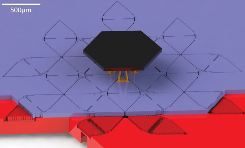
In the MEMS lidar application, a tiny mirror directs a fixed laser beam in multiple directions. The micromirror, moving rapidly due to its low moment of inertia, can execute a two-dimensional scan in a fraction of a second. It can replace the traditional lidar’s bulky scanning component with a chip that measures about 5-mm square and costs on the order of dollars to tens of dollars, developers claim.
In search of a new chip
The ideal MEMS micromirror for lidar is still in development. Existing micromirrors were designed for other applications, such as projection displays or optical switching. They lack lidar’s three simultaneous needs: a large (2-4-mm) micromirror, with a wide (30-60-degrees) angular range of motion, that can pass rigorous automotive testing and validation.
Typical development times and costs for a new custom MEMS device are 18-24 months and $1 million to $3 million to a final prototype. To reach full production, it typically takes three to five years and $10 million to $20 million, experts explain.
Validating MEMS micromirrors for automotive includes, as SAE readers know, meeting many durability and reliability requirements dictated by established standards, such as the AEC-Q100. These include vibration, temperature, humidity, electrical shock, mechanical shock, and chemical resistance. Moreover, the volume of chips is approximately 100M per year, with the quality level at parts-per-million (or lower).

Micromirrors have been in commercial production for more than 20 years. The most development has been in optical switching and displays. Among displays, there are two types, digital and analog.
Digital mirrors switch between only two positions. Analog mirrors have a continuous set of positions.
Analog micromirrors for displays bear the closest resemblance to lidar micromirrors. Like lidar, these MEMS micromirrors have a single mirror that moves in analog fashion in two directions. But, the mirror is smaller (<1 mm) than those typically used in lidar. And perhaps most importantly, display micromirrors were typically engineered for consumer applications, whose qualification requirements are less challenging than for automotive.
Design challenges
There are a multitude of design implications of the increased mirror size and automotive qualification requirements. Automotive temperature ranges are wide (-40°C to +150°C), and mismatches in the coefficient of thermal expansion (CTE) are a common source of device failure. This implies that a mirror which is composed of a single material, such as silicon, will have the lowest failure rates due to CTE mismatch. Mechanical shock and vibrational requirements require that the gimbal designs be able to withstand high forces, reject motion in the unwanted translational and rotational directions, while being pliable enough to rotate about the desired directions.
Automotive humidity requirements require that the device tolerate 0% to 100% humidity. One implication is that the device must tolerate water droplets. A common cause of failure in MEMS devices is “stiction,” which occurs when the moving parts of a MEMS device stick to the stationary parts. When this happens, the moving parts can no longer move, and the MEMS device no longer functions.
The surface tension of a water droplet can bridge small gaps in the MEMS chips. As the water droplet evaporates, it draws together the two sides of the gap, stick them together, and the micromirror is unable to scan. To prevent this, one method is to avoid small gaps in the design, which electrostatic actuation typically requires. Another method is to reduce the droplet’s surface tension with a chemical treatment often used in MEMS microphones. Hermetic packaging is a third solution for keeping moisture out. These methods may be combined to work together to increase overall reliability.
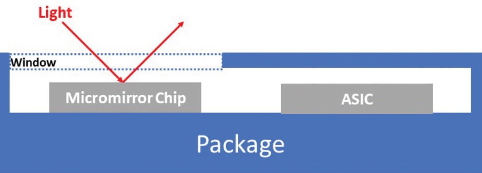
Electronics and software communicate with the system and monitor and control the mirror. The electronics are typically embodied in the ASIC (Application Specific Integrated Circuit) and are packaged together with the MEMS chip. The ASIC is mixed-signal and has a digital portion for programmable command and communication with the system and an analog section for direct control and readout of the mirror.
The ASIC needs to be engineered for automotive qualification to tolerate adverse conditions such as water intrusion, electrical shock, and electromagnetic engine noise.
MEMS lidar packaging and test
After silicon chips are fabricated, they are placed into “packaging” that protects the chip from the environment, while allowing electrical and optical signals to pass to and from the MEMS micromirror. The packaging is a critical part of all MEMS devices, particularly so for automotive applications, since it will protect the MEMS device from water, dirt, oil, particles, and other contaminants that can cause the device to fail.
While the packaging protects the MEMS chip, it can also adversely affect the chip. Many MEMS device failures are associated with the packaging. For example, packages are typically made of ceramic, metal, and/or plastic, and over an automobile’s wide temperature range there can be a strong CTE mismatch between the package and the silicon chip. This can cause inaccuracies, errors, and outright failures.
Ceramic packages have the closest CTE match to silicon but are the most expensive. Plastic packages are the most cost effective but have the largest CTE mismatch and cannot hermetically protect the MEMS device. The cost sensitivity of consumer applications requires that they use plastic packaging, and many of the techniques used in those applications can be adapted to manage the CTE mismatch for automotive applications.
After the chip is packaged, the device is calibrated and tested to ensure that it meets requirements. With approximately 100 million automobiles produced every year, testing every device is time consuming and costly. As a result, efficient testing requires a strategy that tests devices at multiple points in the manufacturing process, as well as custom test capabilities that can evaluate every device efficiently.
Charles Chung, Ph.D., has over 25 years of experience with MEMS devices and microsystems. He is a member of the University of Pennsylvania’s Singh Nanotechnology Center’s Advisory Board, and a recipient of the Gates Global Grand Challenges Grant. He has developed multiple MEMS devices, including wireless sensor nodes, DNA sequencing chips, microphones, gyroscopes, accelerometers, and pressure sensors.
More From SAE Media Group
Sensing Technology
Processing and Packaging MEMS to Maximize Functionality
Autonomous Vehicle Engineering
Velodyne Preps for Volume Lidar
Photonics & Imaging Technology
Leap in Lidar Could Improve Safety and Security of New Technology
Sensor Technology
2021 Supplier Guide: Sensors
Tech Briefs
Packaging for SiC Sensors and Electronics
Sensor Technology
New Products
Tech Briefs
5 Ws of 3D-Printed MEMS
Electronics & Sensors INSIDER
Integrating Dimensions to Get More Out of Moore’s Law
Aerospace & Defense Tech Briefs
MEMS-Based Accelerometer to Measure Microgravity for In-Orbit Manufacturing

Motion Design
High-Sensitivity, Low-Noise MEMS Accelerometer
Automotive Engineering
Lumotive’s New LCM Underpins Next-Gen Lidar
Medical Design Briefs
Sensor Packaging: Critical MEMS Considerations
Photonics & Imaging Technology
Why Honda Wants FMCW LiDAR in Next Generation Mobility
Tech Briefs
Rapidly Testing Stretchable Sensors
Tech Briefs
Miniature Lung-Heart Sensor on a Chip
Photonics & Imaging Technology
This MEMS Scanning Mirror Could Solve LiDAR’s Expensive Autonomous Vehicle Challenges
Electronics & Sensors INSIDER
Engineers “Grow” Atomically Thin Transistors on Top of Computer Chips
Tech Briefs
Compact 3D LiDAR Imaging System

Automotive Engineering
MEMS Drive Wants to Shake up Automotive Sensor
Tech Briefs
New on the Market
Tech Briefs
Products of Tomorrow
Electronics & Sensors INSIDER
Graphene Boosts Flexible and Wearable Electronics Boosts
Aerospace & Defense Tech Briefs
Future Advances in Electronic Materials and Processes - Flexible Hybrid Electronics
Electronics & Sensors INSIDER
MIT Team Takes a Major Step Toward Fully 3D-Printed Active Electronics
Sensor Technology
‘Impossible’ Millimeter Wave Sensor Has Wide Potential

Electronics & Sensors INSIDER
This LED Can Be Integrated Directly Into Computer Chips
Electronics & Sensors INSIDER
Opening Up the Potential of Thin-Film Electronics for Flexible Chip Design
Top Stories
INSIDERManufacturing & Prototyping
![]() How Airbus is Using w-DED to 3D Print Larger Titanium Airplane Parts
How Airbus is Using w-DED to 3D Print Larger Titanium Airplane Parts
INSIDERManned Systems
![]() FAA to Replace Aging Network of Ground-Based Radars
FAA to Replace Aging Network of Ground-Based Radars
NewsTransportation
![]() CES 2026: Bosch is Ready to Bring AI to Your (Likely ICE-powered) Vehicle
CES 2026: Bosch is Ready to Bring AI to Your (Likely ICE-powered) Vehicle
NewsSoftware
![]() Accelerating Down the Road to Autonomy
Accelerating Down the Road to Autonomy
EditorialDesign
![]() DarkSky One Wants to Make the World a Darker Place
DarkSky One Wants to Make the World a Darker Place
INSIDERMaterials
![]() Can This Self-Healing Composite Make Airplane and Spacecraft Components Last...
Can This Self-Healing Composite Make Airplane and Spacecraft Components Last...
Webcasts
Defense
![]() How Sift's Unified Observability Platform Accelerates Drone Innovation
How Sift's Unified Observability Platform Accelerates Drone Innovation
Automotive
![]() E/E Architecture Redefined: Building Smarter, Safer, and Scalable...
E/E Architecture Redefined: Building Smarter, Safer, and Scalable...
Power
![]() Hydrogen Engines Are Heating Up for Heavy Duty
Hydrogen Engines Are Heating Up for Heavy Duty
Electronics & Computers
![]() Advantages of Smart Power Distribution Unit Design for Automotive...
Advantages of Smart Power Distribution Unit Design for Automotive...
Unmanned Systems
![]() Quiet, Please: NVH Improvement Opportunities in the Early Design...
Quiet, Please: NVH Improvement Opportunities in the Early Design...