


SOI ‘Sauce’ for Next-gen Microelectronics
Fully depleted silicon-on-insulator semiconductor is a mouth full, but FD-SOIs are vital for meeting the performance specs of automated vehicles and the IoT.

Automotive applications and the Internet of Things (IoT) will be the next big drivers for semiconductor growth through 2025. Vehicles are increasingly relying on greater intelligence, simultaneous connectivity and sophisticated, reliable electronics. Today many vehicles have on-board systems that monitor conditions, alert the driver and even automate some functions (SAE Levels 2 and 3) to enhance driving safety, avoid human error and protect pedestrians.

In the future, these features will be extended to create fully autonomous SAE Level 5 vehicles. To cost-efficiently mass produce these vehicles, the adoption of secure, reliable, high-performance and low-power microelectronics is essential.
Designing and managing automotive electronic systems to execute advanced functions in mobility mode will depend heavily on complex semiconductor circuits and advanced components such as a variety of sensors, microprocessors, microcontrollers and mixed- signal analog/radio-frequency (RF) ICs. These micro- electronic components must operate on low power and have superior reliability in harsh environments while delivering high performance; fast data-transfer rates; simultaneous, multi-point connectivity; and the cost effectiveness to be implemented in all vehicles.
FD-SOI with body biasing
Fully depleted silicon-on-insulator (FD-SOI) semi-conductor technology enables scalable, planar semi-conductors with key advantages over ICs made with bulk-silicon technology. Body- or back-bias is one of the benefits of chips manufactured on FD-SOI substrates. It serves as an adjustable dial that allows the chips to run faster when required or to be more energy efficient when performance is not as critical.
This unique feature was demonstrated for ultra-low-power microcontrollers in Japan and manufactured by Renesas. This versatility means that FD-SOI can be used to create on-board automotive systems capable of higher performance, greater energy efficiency and superior reliability.
FD-SOI’s back-bias enables threshold voltage (Vt) tuning for better performance/power trade-off and variability control. The principle of body biasing is well known in bulk silicon technologies, but as transistor sizes are scaled smaller than the 40-nm node, body biasing becomes much less efficient, especially for the three-dimensional device architecture known as FinFET. With planar FD-SOI technology, the presence of a buriedoxide (BOx) layer within the semiconductor wafer and back-gate isolation enables high efficiency and extension of the back-bias voltage range up to -2V/+2V without degrading the drive current (Ion) and off-state current (Ioff ) universal relationship and their distribution.
Thanks to this extended range, body bias can improve circuit performance up to 200% or reduce leakage power by one decade. This is a major differentiator for FD-SOI compared with planar bulk and FinFET technologies. It provides an additional way to reach optimal energy efficiency.
As semiconductor feature sizes are reduced, thermal management becomes an issue. Planar FD-SOI devices with thin BOx layers demonstrate much lower thermal resistance than FinFET. The larger self-heating effect in FinFETs results in lower reliability, prolonged gate delays, increased power leakage and higher overall chip development costs.
Reliability benefits

Adaptive voltage scaling (AVS) is the most common low-power technique used in CMOS technologies to compensate for variability, reduce power consumption or boost performance by modulating the voltage supply. Another technique unique to FD-SOI, called adaptive body biasing (ABB), can be applied by simply modulating the back-gate voltage in a static or dynamic way during application runtime. The combination of both techniques provides outstanding results such as 36% speed gain or 50% power savings on high-performance applications compared to all other CMOS technologies.
Additionally, FD-SOI is more than 25 times more resilient to soft error rates (SER) than bulk silicon. At the circuit design level, this means that FD-SOI requires less error correction and redundancy, making the design much simpler and less power consuming.
Body biasing also offers tremendous help in variability control. In advanced semiconductor technologies below the 45-nm node, variability has become a key concern due to increasing process complexity.
For leakage-driven ADAS and infotainment products, STMicroelectronics and NXP Semiconductors developed an innovative built-in body-bias methodology to fulfill customer requirements. It incorporates body biasing in all design stages, from synthesis to engineering. This strategy enables significant improvements including a 30% reduction in static power as well as 4X frequency and 2X leakage spread reductions.
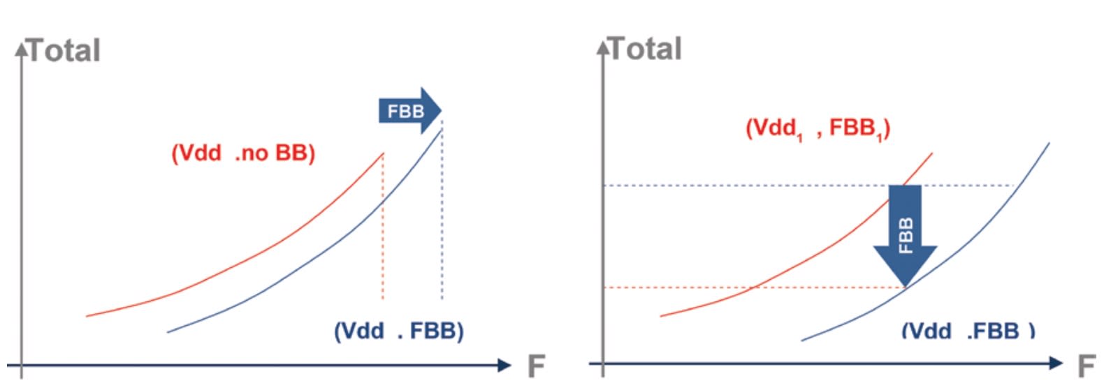
The body-biasing-based process compensation technique also allows chip designers to take full control of the minimum voltage (Vmin) by reducing it several tenths of a millivolt and making it independent of the process corner. This results in significant dynamic power reduction and reliability improvement by scaling Vdd. As shown in the graph on p.31, with the process, temperature and aging compensation capability, FD-SOI guarantees a high level of robustness at <1 ppm to meet automotive safety requirements.
5G connectivity for smart cars
In addition to ADAS, enabling technologies to realize the Level 5 vehicle include high-data-rate communications for vehicle-to-everything (V2X) and in-car data transfer. Fifth-generation (5G) connectivity presents three main benefits: faster speed, lower latency and increased bandwidth.

FD-SOI technologies provide not only high performance, but also the lowest power consumption solutions for any RF or mmWave transceivers. This is due to having low gate resistance and parasitic capacitance that is at least 30% lower than other bulk CMOS approaches. The 65-22-nm FD-SOI-based technologies are already qualified for high-volume manufacturing by Renesas, STMicroelectronics, Samsung and GlobalFoundries. A 22nm FD-SOI can provide nearly twice the performance (Ft and Fmax) of a 14-nm FinFET at lower cost per square millimeter of real estate due to the intrinsic properties of the planar, thin undoped body and the total isolated device structure with a gate-first approach.
More importantly, using body-bias RF transceivers can retain high Ft and Fmax at lower operation voltage for reducing dynamic power consumption.
FD-SOI is well suited for automotive applications with its low active and static power, better performance/power trade-off, cost effectiveness, high-performance analog/ RF co-integration and—most importantly—better reliability, lower self-heating and lower leakage at the high temperatures faced in automotive electronics operations. A wide range of companies including NXP Semiconductor, Mobileye and Renesas have shown FD-SOI to be a viable ultra-low-power IC candidate for IoT, ADAS and autonomous automotive applications.
FD-SOI’s full body-bias capability offers outstanding performance, power, reliability and cost advantages while leveraging mature planar design and manufacturing processes to accelerate time to market. FD-SOI-based devices are available today and will continue improving in performance, density and integration levels to provide cost-effective solutions for global automotive markets.
Bich-Yen Nguyen is a Senior Fellow at Soitec supporting the tech- nology development of new device fields and applications. She holds over 140 worldwide patents and has authored more than 150 technical papers on IC process, integration and device technologies.
Philippe Flatresse, Ph.D, Soitec’s Business Development Manager, is a pioneer of SOI technology and demonstrated its key advantages for low power/high performance digital applications. A microelectronics engineer, he has authored or co-authored more than 70 technical papers in advanced CMOS technologies.
More From SAE Media Group
Photonics & Imaging Technology
Photonic Communication Comes to Computer Chips
Tech Briefs
Ultra-Wide-Bandgap Power Electronics
Aerospace & Defense Tech Briefs
New 3D Chips Could Make Electronics Faster and More Energy-Efficient
Tech Briefs
Thin-Film Electronics for Flexible Chip Design
Tech Briefs
Nanotransistors Stay Cool at High Voltages
Electronics & Sensors INSIDER
Opening Up the Potential of Thin-Film Electronics for Flexible Chip Design
Autonomous Vehicle Engineering
Accelerating Automotive Radar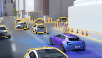
Motion Design
High-Sensitivity, Low-Noise MEMS Accelerometer
Embedded Technology INSIDER
New Circuits Can Function at Temperatures Above 650°F


Electronics & Sensors INSIDER
Brain-Inspired Highly Scalable Neuromorphic Hardware

Electronics & Sensors INSIDER
Engineers “Grow” Atomically Thin Transistors on Top of Computer Chips

Battery & Electrification Technology
Micro-Supercapacitors Enable Fast Charging
Medical Design Briefs
Integrating Smart Technology into Wearable Device Design
Electronics & Sensors INSIDER
Integrating Dimensions to Get More Out of Moore’s Law

Automotive Engineering
Chipping in to Get More From Battery Packs
Tech Briefs
Executive Forum: Sensors & the IoT

Tech Briefs
Pyroelectric Sandwich Thermal Energy Harvester
Tech Briefs
Software-Connected Wafer Level Reliability Test
Photonics & Imaging Technology INSIDER
STARLight Project Launches European Value Chain for Silicon Photonics Production
Top Stories
INSIDERManufacturing & Prototyping
![]() How Airbus is Using w-DED to 3D Print Larger Titanium Airplane Parts
How Airbus is Using w-DED to 3D Print Larger Titanium Airplane Parts
INSIDERManned Systems
![]() FAA to Replace Aging Network of Ground-Based Radars
FAA to Replace Aging Network of Ground-Based Radars
NewsTransportation
![]() CES 2026: Bosch is Ready to Bring AI to Your (Likely ICE-powered) Vehicle
CES 2026: Bosch is Ready to Bring AI to Your (Likely ICE-powered) Vehicle
NewsSoftware
![]() Accelerating Down the Road to Autonomy
Accelerating Down the Road to Autonomy
EditorialDesign
![]() DarkSky One Wants to Make the World a Darker Place
DarkSky One Wants to Make the World a Darker Place
INSIDERMaterials
![]() Can This Self-Healing Composite Make Airplane and Spacecraft Components Last...
Can This Self-Healing Composite Make Airplane and Spacecraft Components Last...
Webcasts
Defense
![]() How Sift's Unified Observability Platform Accelerates Drone Innovation
How Sift's Unified Observability Platform Accelerates Drone Innovation
Automotive
![]() E/E Architecture Redefined: Building Smarter, Safer, and Scalable...
E/E Architecture Redefined: Building Smarter, Safer, and Scalable...
Power
![]() Hydrogen Engines Are Heating Up for Heavy Duty
Hydrogen Engines Are Heating Up for Heavy Duty
Electronics & Computers
![]() Advantages of Smart Power Distribution Unit Design for Automotive...
Advantages of Smart Power Distribution Unit Design for Automotive...
Unmanned Systems
![]() Quiet, Please: NVH Improvement Opportunities in the Early Design...
Quiet, Please: NVH Improvement Opportunities in the Early Design...