


Accelerating Automotive Radar
NXP’s new fifth-generation chipsets unleash 16-nm FinFet technology to the ADAS and AV markets.

Radars that are a key sensing element of automated driver-assistance systems (ADAS) are evolving at a rapid pace. Far removed from the blip-on-a-screen radars of ancient war movies, they’re now engineered to cater to a variety of OEM use cases and the need for both higher performance and reduced cost.
“It’s not possible to use a one-size-fits-all radar sensor, whether it be a corner sensor for NCAP and NHTSA safety requirements such as automated emergency braking or blind-spot detection, or a front long-range sensor,” explained Matthias Feulner, senior director, ADAS, at NXP Semiconductors. “Scalability of chipsets is now critical, because it allows for tailoring for the individual use case and not just for a single niche application. It ties directly to the needs of vehicle OEMs that have a range of requirements across their brand and model portfolios.”

Automotive is witnessing what Feulner calls a “triple acceleration” of the radar sensor market. According to NXP, in 2020 there was an average of one radar sensor per vehicle; that will increase within a few years to five or more sensors per vehicle – perhaps four corner radars, a front radar and maybe a rear-facing radar for rear collision avoidance. The trend is occurring entirely within the ADAS space, up to and including SAE Level 3. He said there is growing demand from OEMs for the so-called “Level 2+” automated-driving systems that support a growing list of safety-and-comfort features such as 360-degree surround sensing and higher-performance/higher-resolution sensors that support systems like GM’s Super Cruise. OEMs are increasingly offering such systems in upper-range cars and light trucks to optimize the driving experience and to differentiate their brands and model ranges.
“The Level 2+ comfort features offer [SAE] Level 3 autonomy capabilities without the liabilities associated with the higher levels of autonomy, because the driver still needs to keep hands on the wheel,” Feulner said. He added that NXP also sees mobility-as-a-service (MaaS) applications, including robotaxis and delivery services, “where cost sensitivity isn’t as acute as in typical passenger cars,” as another important market.
NXP’s recently launched, fifth-generation radar system solution for dedicated automotive use leverages the company’s experience in radar-signal processing and hardware (see sidebar). Currently, all of the top 15 automotive OEMs are using NXP radar chipsets, according to Feulner. The company was a pioneer in introducing deep submi-cron CMOS (complementary metal-oxide-semiconductor) technology in automotive sensors. Deep submicron refers to transistors sized below 0.35um, with faster switching rates, increased power density and cost efficiency.
New 4D imaging radar

Imaging radars significantly enhance a vehicle’s sensing capabilities. Operating in the 77 GHz frequency range, imaging radars enable very precise mapping and environmental awareness, thus improving object detection and separation. They deliver higher-fidelity object classification – the ability to accurately identify an object as a bike, a car, a truck, an animal or a pedestrian, for example. NXP’s latest 4D imaging radar uses additional enhancements such as “virtual antennae” that directly correlate to sensor resolution. “Our imaging radar uses cascaded radar front ends to create as many as 192 of the virtual antennae which, along with greatly enhanced signal-processing capability, allows simultaneous sensor functions such as digital beam-forming.”
NXP claims its recently introduced 4D imaging radar can detect objects at more than 300-meters (984-ft) range in long-range mode and simultaneously producing high-resolution point-cloud output in short-range mode. “It is significant for Level 2+ use cases such as auto-pilot systems and lane-keep assist, and for full autonomy at Levels 3 through 5,” Feulner said. The radar is capable of up to 16X enhancement in angular resolution to <1 degree, through a combination of the 192-virtual-antennae system and digital-algorithm post processing. A linear algebra radar accelerator provides up to 64 times better performance compared to an ARM Cortex A53 microarchitecture, claims NXP. The radar’s optimized processor “reduces implementation cost and power consumption by up to 50% compared to general purpose FPGAs [field-programmable gate array, a programmable electronic device that uses digital logic circuitry],” he said.
A 16-nm first
According to Feulner, NXP early in its radar developments transitioned from the older 24 GHz systems that were often built on silicon-germanium technology toward 77 GHz radars based on 40nm RF-CMOS technology; RF CMOS is a metal–oxide–semiconductor (MOS) integrated circuit (IC) that integrates radio-frequency (RF), analog and digital electronics on a mixed-signal CMOS (complementary MOS) RF circuit chip.
“The transition allowed for higher sensor resolution while allowing for a smaller physical foot-print and more cost-efficient sensors,” he explained. “With our first-generation devices, NXP was first to ramp RF-CMOS technology into automotive volume production. Our latest generation provides more sensing range and more scalability across use cases and allows more ‘cascadability’ to connect more sensor front ends for higher sensor resolution.”
NXP’s new fifth-generation radars are claimed to be the first to take to market dedicated automotive radar microcontrollers in a 16-nm FinFet technology. A fin field-effect transistor (FinFET) is a multigate MOSFET (metal-oxide-semiconductor field-effect transistor) device built on a substrate where the gate is placed on two to four sides of the channel or wrapped around the channel. This forms a double gate structure. The generic name “finfets” comes from the source/drain region that forms fins on the silicon surface. FinFET devices are claimed to offer significantly faster switching times and higher current density than planar CMOS (complementary metal-oxide-semiconductor) technology.
The FinFet design “brings significant power-consumption savings and performance per watt, with faster processing,” Feulner claimed. “This is important because the radar sensors are often mounted behind the front bumper, where thermal management tends to be a challenge.”
More From SAE Media Group
Aerospace & Defense Tech Briefs
New 3D Chips Could Make Electronics Faster and More Energy-Efficient
Automotive Engineering
Single-chip digital imaging radar heads for 2022 production
Tech Briefs
Thin-Film Electronics for Flexible Chip Design
Electronics & Sensors INSIDER
Opening Up the Potential of Thin-Film Electronics for Flexible Chip Design
Electronics & Sensors INSIDER
A New Kind of Transistor — A Conductive Polymer
Tech Briefs
Q&A: Radar Imaging at Terahertz Frequencies
Aerospace & Defense Tech Briefs
New Products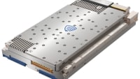
Autonomous Vehicle Engineering
SOI ‘Sauce’ for Next-gen Microelectronics
Autonomous Vehicle Engineering
Opsys Tech Demos Cost-Effective Solid-State Lidar-Module Prototypes
Tech Briefs
How Much Do You Know About Integrated Circuits?
Defense INSIDER
Defense Leaders Receive First Intel SHIP Multi-Chip Prototype
Electronics & Sensors INSIDER
Brain-Inspired Highly Scalable Neuromorphic Hardware
Off-Highway Engineering
Uhnder and Spartan to Partner on Hi-rez RadarAutomotive Engineering
Expanding ADAS Roles for Radar and Cameras
Aerospace & Defense Tech Briefs
Miniaturized Rad-Hard System Reduces Electronics Footprint
Tech Briefs
“One-Way” Electronic Devices

Tech Briefs
Graphene “Nano-Origami” Creates Tiny Microchips
Electronics & Sensors INSIDER
Engineers “Grow” Atomically Thin Transistors on Top of Computer Chips
Tech Briefs
New on the Market
Electronics & Sensors INSIDER
Next-Gen Automotive Semiconductors Are Critical for Level 5 Driverless Cars
Photonics & Imaging Technology INSIDER
STARLight Project Launches European Value Chain for Silicon Photonics Production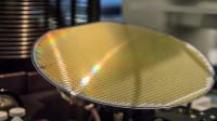
Electronics & Sensors INSIDER
MIT Engineers Grow “High-Rise” 3D Chips
Automotive Engineering
Aluminum Cooling Solutions for EV Power Electronics
Automotive Engineering
Semiconductor Maker Infineon Buys Rival International Rectifier
Aerospace & Defense Tech Briefs
FPGAs and HPC
Automotive Engineering
The Path to Better, Smarter Vehicle Charging
Top Stories
INSIDERDefense
![]() New Raytheon and Lockheed Martin Agreements Expand Missile Defense Production
New Raytheon and Lockheed Martin Agreements Expand Missile Defense Production
NewsAutomotive
![]() Ford Announces 48-Volt Architecture for Future Electric Truck
Ford Announces 48-Volt Architecture for Future Electric Truck
INSIDERManufacturing & Prototyping
![]() Active Strake System Cuts Cruise Drag, Boosts Flight Efficiency
Active Strake System Cuts Cruise Drag, Boosts Flight Efficiency
ArticlesTransportation
![]() Accelerating Down the Road to Autonomy
Accelerating Down the Road to Autonomy
INSIDERMaterials
![]() How Airbus is Using w-DED to 3D Print Larger Titanium Airplane Parts
How Airbus is Using w-DED to 3D Print Larger Titanium Airplane Parts
Road ReadyTransportation
Webcasts
Electronics & Computers
![]() Cooling a New Generation of Aerospace and Defense Embedded...
Cooling a New Generation of Aerospace and Defense Embedded...
Power
![]() Battery Abuse Testing: Pushing to Failure
Battery Abuse Testing: Pushing to Failure
Connectivity
![]() A FREE Two-Day Event Dedicated to Connected Mobility
A FREE Two-Day Event Dedicated to Connected Mobility
Automotive
![]() Quiet, Please: NVH Improvement Opportunities in the Early Design Cycle
Quiet, Please: NVH Improvement Opportunities in the Early Design Cycle
Transportation
![]() Advantages of Smart Power Distribution Unit Design for Automotive &...
Advantages of Smart Power Distribution Unit Design for Automotive &...
Aerospace
![]() Sesame Solar's Nanogrid Tech Promises Major Gains in Drone Endurance
Sesame Solar's Nanogrid Tech Promises Major Gains in Drone Endurance