


Lasing Consequences of Silicon Nanostructures
This research could have implications in removing data transmission bottlenecks.
While silicon electronics has been a success in modem technologies, silicon photonics is still in development and in need of a laser source. Many approaches have been explored, from anodized silicon luminescence, to generating direct emissions by quantum-confinement, and to indirect down-conversion of a shorter wavelength laser light via silicon's nonlinear dielectric responses. One approach that was developed has led to the demonstration of laser emission in silicon-on-insulator at cryogenic temperatures (<85K).
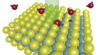
Silicon's inability to emit light and to 'lase' is rooted in the particular atomic arrangement (lattice) of silicon atoms in their crystalline form. As such, the creation of an all-silicon laser or merely an efficient all-silicon light emitter would necessarily begin at the atomic level. Emissive deformation centers (or 'designer defects') were created in the silicon lattice. These emissive centers exist naturally in silicon. In electronics, they are either detrimental to device performance or are a source of unwanted variation.
One example of such centers is called the G-center, which is formed by moving a silicon atom from its normal lattice site and substituting a carbon atom in its place. When the substituted carbon pairs up with a second carbon atom nearby, a local lattice deformation or emissive center is created and an electron captured at the site can then emit light directly. One way to make silicon more optically active is to increase the density of these G-centers, without adversely increasing electrical and optical losses, so as to allow laser action.
A nano-patterning technique was developed that uses an etch mask made of a regular array of oxide (AAO). In the etching process, this AAO mask is placed directly on a slice of silicon. The etching through the mask results in a pattern of silicon structures. The extreme uniformity of the approach helped to keep optical losses low, the large field size provided sufficient total optical gain, the small feature sizes minimized scattering loss, and the hardness of the AAO stood up well against the deep etching process and protected the underlying silicon everywhere except where the nano-pores were to be etched.
The same nano-patterned etching pro - cess also created local lattice deformation and strain field in the side-wall region (-4 nm thick) and a band-gap narrowing. Both benefited optical emission by facilitating the gathering of electron-hole pairs from the surrounding silicon to the emission centers in the side-wall layer of the etched pore. This itself also benefited from the fact that the nano-pores are much closer together than the electron diffusion length within crystalline silicon.
A future option is to combine patterned implantation with the strain effects that can aid in optical activity, both through direct lattice deformation and indirect selection and stabilization of the desired emissive deformation centers.
This work was done by Jimmy Xu of Brown University for the Office of Naval Research.
ONR-0012
This Brief includes a Technical Support Package (TSP).
Lasing Consequences of Silicon Nanostructures
(reference ONR-0012) is currently available for download from the TSP library.
Don't have an account?
More From SAE Media Group
Photonics & Imaging Technology
Using Magnets to Toggle Nanolasers Leads to Better Photonics

Aerospace & Defense Tech Briefs
On the Pulsed Laser Ablation of Metals and Semiconductors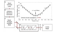
Aerospace & Defense Tech Briefs
Advances in Materials for Photonic Applications
Photonics & Imaging Technology
A Sharper Look at the Interior of Semiconductors
Photonics & Imaging Technology
Nanoscale Machines Convert Light into Work
Tech Briefs
Low-Energy Nanolaser Shines in all Directions
Photonics & Imaging Technology
Continuous and Stable Lasing Achieved From Low-Cost Perovskites at Room Temperature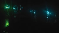
Photonics & Imaging Technology
A First-Of-Its-Kind Integrated Optical Isolator
Medical Design Briefs
Scientists Create Continuously Emitting Microlasers With Nanoparticle-Coated Beads
Tech Briefs
Nanoscale LED Also Functions as a Laser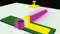
Photonics & Imaging Technology
A Laser That Could Reshape the Landscape of Integrated Photonics
Aerospace & Defense Tech Briefs
3D Meta-Optics for High-Energy Lasers
Aerospace & Defense Tech Briefs
Analysis of Broadband Metamaterial Shielding for Counter-Directed Energy Weapons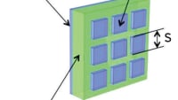
Air Force Research Laboratory Technology Horizons
Patterned Gallium Arsenide Devices for Infrared Countermeasures
Photonics & Imaging Technology
Ultrafast Beam-Steering Breakthrough at Sandia Labs
Tech Briefs
5 Ws of Invisible Glass
Photonics & Imaging Technology
Individual Quantum Dots Imaged in 3-D for the First Time
Photonics Tech Briefs
Pulsed Laser System to Simulate Effects of Cosmic Rays in Semiconductor Devices
Photonics Tech Briefs
DFM Your Device? Simulation Is the Answer
Photonics & Imaging Technology
2.2-Micron, Uncooled, InGaAs Photodiodes and Balanced Photoreceivers up to 25-GHz Bandwidth
Photonics & Imaging Technology
Researchers Generate Terahertz Laser with Laughing Gas
Medical Design Briefs
Nanotechnology Developments Drive the Future of BIOPHOTONICS
Tech Briefs
Optical Device Fine-Tunes the Color of Light
Photonics & Imaging Technology
How to Innovate and Overcome the Challenges of Blue Laser Beam Shaping
Photonics & Imaging Technology
Making Measurements with a Fine-Toothed Comb

Tech Briefs
High-Power, Portable Terahertz Laser
Tech Briefs
Material Increases Efficiency of LED Devices
Overview
The document presents a comprehensive report on advancements in silicon nanostructures and their potential for laser emission, primarily authored by Jimmy Xu and his team at Brown University. The research focuses on overcoming silicon's inherent limitations in light emission, which stem from its atomic arrangement in crystalline form. The report outlines the successful achievement of optically pumped laser emission at cryogenic temperatures (below 85K) using carbon-implanted nano-patterned silicon-on-insulator substrates.
Key methodologies employed in the research include ion implantation and solid-phase epitaxy for recrystallization, which resulted in a remarkable 30-fold improvement in luminescence intensity. The nano-patterning was achieved through reactive-ion-etching, utilizing an anodized aluminum oxide membrane as a mask. These techniques are crucial for enhancing the optical properties of silicon, making it a viable candidate for laser applications.
The document emphasizes the significance of these findings, suggesting that the ability to create silicon lasers could lead to innovative devices and applications that have not yet been conceived. Potential benefits include improved optical and electronic integration, which could alleviate data transmission bottlenecks within computer chips and facilitate the mass production of low-cost micro-gadgets. These gadgets could utilize infrared light emitted from silicon chips for medical diagnostics, showcasing the practical implications of the research.
Additionally, the report includes a list of publications and awards related to the research, highlighting the contributions of various authors and their collaborative efforts in advancing the field. The findings lay a solid foundation for future research aimed at achieving room-temperature lasing in silicon, which would represent a significant milestone in the development of silicon-based optoelectronic devices.
In summary, this document encapsulates a pivotal moment in silicon nanotechnology, illustrating the potential for silicon to serve as an emissive optical medium. The research not only addresses the challenges associated with silicon's light emission but also opens avenues for future innovations in laser technology and integrated photonics.
Top Stories
INSIDERDesign
![]() How Airbus is Using w-DED to 3D Print Larger Titanium Airplane Parts
How Airbus is Using w-DED to 3D Print Larger Titanium Airplane Parts
NewsSensors/Data Acquisition
![]() Microvision Aquires Luminar, Plans Relationship Restoration, Multi-industry Push
Microvision Aquires Luminar, Plans Relationship Restoration, Multi-industry Push
INSIDERManned Systems
![]() A Next Generation Helmet System for Navy Pilots
A Next Generation Helmet System for Navy Pilots
NewsAR/AI
![]() Accelerating Down the Road to Autonomy
Accelerating Down the Road to Autonomy
INSIDERDefense
![]() New Raytheon and Lockheed Martin Agreements Expand Missile Defense Production
New Raytheon and Lockheed Martin Agreements Expand Missile Defense Production
ArticlesAR/AI
![]() CES 2026: Bosch is Ready to Bring AI to Your (Likely ICE-powered) Vehicle
CES 2026: Bosch is Ready to Bring AI to Your (Likely ICE-powered) Vehicle
Webcasts
Semiconductors & ICs
![]() Advantages of Smart Power Distribution Unit Design for Automotive...
Advantages of Smart Power Distribution Unit Design for Automotive...
Unmanned Systems
![]() Quiet, Please: NVH Improvement Opportunities in the Early Design...
Quiet, Please: NVH Improvement Opportunities in the Early Design...
Electronics & Computers
![]() Cooling a New Generation of Aerospace and Defense Embedded...
Cooling a New Generation of Aerospace and Defense Embedded...
Automotive
![]() Battery Abuse Testing: Pushing to Failure
Battery Abuse Testing: Pushing to Failure
Transportation
![]() A FREE Two-Day Event Dedicated to Connected Mobility
A FREE Two-Day Event Dedicated to Connected Mobility