


AC Coupled Interconnect for Low-Power Spaceborne Electronics
This technology could reduce the power consumed in high-speed memory buses.
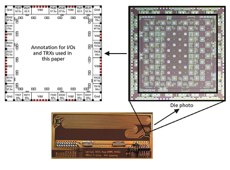
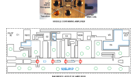
An AC coupled interconnect (ACCI) has been developed that could be used to create multiple solutions to contactless chip-to-chip communications. Assembly and testing of a 0.18 um bulk CMOS chip containing multiple circuit experiments were performed. Figure 1 shows the chip floorplan, chip layout for the wire bonded experiments, and a microscope photograph of the die. The experiments tested in this phase of measurements were located around the periphery of the die in the band designated in the die photo of Figure 1.
A 6-bit wide ACCI bus was demonstrated, which operates at 36 Gbps or 6 Gbps/channel, over 30-cm transmission lines on FR4, with transceiver power dissipation less than 2 mW/Gbps, while subject to crosstalk and switching noise from the simultaneous operation of six channels. Additional signal integrity analysis was performed to ensure it was robust to crosstalk noise and simultaneous switching noise.
Two different inductively coupled systems were designed, one for single-coupled systems, and another for dual-coupled systems. Several versions of the circuits for this structure are currently in IC, MCM, and laminate fabrication. An integrated process structure was developed that can be used to build capacitively coupled laminate packages. The key enabling technology for this structure is a patternable high-K material that can be cured at the same process temperature as solder bumps. Different versions of the material can be cured to match the reflow profile for both leaded and lead-free solder.
Capacitive coupling with the capacitor formed between the chip and a package was demonstrated. Chips were built in a 0.35-μm process and flipped to an MCM substrate. The chips can communicate with each other at 2.5 Gbps over a 5-cm transmission line. Pad sizes down to 70-μm pitch were demonstrated.
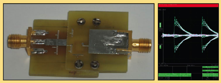
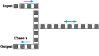
Inductively coupled circuits communicating vertically through a 3D chip-stack were demonstrated. This chip was built in a 0.35-μm process and operated at 2 GHz. Communication was possible with a chip thickness of up to 120 mm. An inductively coupled connector, prototyped in a PCB technology, was demonstrated to operate at 250 MHz. Figure 2 shows a prototype and an eye diagram.
This work was done by Paul D. Franzon of North Carolina State University for the Air Force Research Laboratory. AFRL-0115
This Brief includes a Technical Support Package (TSP).
AC Coupled Interconnect for Low-Power Spaceborne Electronics
(reference AFRL-0115) is currently available for download from the TSP library.
Don't have an account?
More From SAE Media Group


Tech Briefs
How Much Do You Know About Integrated Circuits?
Defense INSIDER
Defense Leaders Receive First Intel SHIP Multi-Chip Prototype

Tech Briefs
Graphene “Nano-Origami” Creates Tiny Microchips
Tech Briefs
Single Event Upset Suppression System (SEUSS)
Tech Briefs
164-GHz MMIC HEMT Frequency Doubler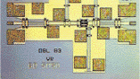


Electronics Tech Briefs
Microelectromechanical SPDT Switches


Tech Briefs
Silicon Carbide High-Voltage Switch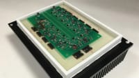
Medical Design Briefs
PCB Microelectronics Assembly Takes Center Stage for Medical Miniaturization
Tech Briefs
SEU-Tolerant Flip-Flops
Motion Design INSIDER
Smart Microrobots Walk Autonomously
Aerospace & Defense Tech Briefs
Silicon Carbide Junction Field-Effect Transistor Devices for Scalable Solid-State Circuit Breakers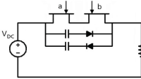
Medical Design Briefs
New Isolated Power Supply Chip Design Improves Efficiency
Overview
The document is a final report on a research project titled "AC Coupled Interconnect for Low Power Spaceborne Electronics," conducted from May 20, 2003, to September 30, 2006. The primary objective of the project was to establish that AC Coupled Interconnect (ACCI) could facilitate contactless chip-to-chip communications, which is crucial for low-power electronics used in space applications.
The report outlines the experimental approach taken to achieve this goal, detailing various demonstrations and results. Key achievements include the design and testing of an FPGA interface/controller for an AFRL space mission, and the successful demonstration of capacitive coupling between chips. Chips were fabricated using a 0.35 μm process and were able to communicate at speeds of 2.5 Gbps over a 5 cm transmission line, showcasing the effectiveness of the technology.
Additionally, the report highlights a contactless 3D chip stack demonstration, where inductively coupled circuits communicated vertically through a 3D chip stack, operating at 2 GHz with a chip thickness of up to 120 mm. This innovation represents a significant advancement in chip communication technology.
The report also discusses the results of experiments conducted with a 0.18 μm bulk CMOS chip, which included a 6-bit wide ACCI bus operating at 36 Gbps (6 Gbps per channel) over 30 cm transmission lines. The experiments demonstrated low power dissipation of less than 2 mW/Gbps, even in the presence of crosstalk and switching noise, indicating robust performance under challenging conditions.
Furthermore, the document describes the design of two different inductively coupled systems—single and dual coupled systems—illustrating the circuit diagrams for both. The report emphasizes the importance of signal integrity analysis to ensure reliable operation amidst noise.
In summary, the report encapsulates the successful outcomes of the ACCI project, including technological advancements in capacitive and inductive coupling for chip communications, and outlines the potential for future applications in spaceborne electronics. It also lists the papers published, students graduated, and technology transfer outcomes resulting from the research, underscoring the project's impact on the field.
Top Stories
INSIDERDefense
![]() New Raytheon and Lockheed Martin Agreements Expand Missile Defense Production
New Raytheon and Lockheed Martin Agreements Expand Missile Defense Production
NewsAutomotive
![]() Ford Announces 48-Volt Architecture for Future Electric Truck
Ford Announces 48-Volt Architecture for Future Electric Truck
INSIDERManufacturing & Prototyping
![]() Active Strake System Cuts Cruise Drag, Boosts Flight Efficiency
Active Strake System Cuts Cruise Drag, Boosts Flight Efficiency
ArticlesTransportation
![]() Accelerating Down the Road to Autonomy
Accelerating Down the Road to Autonomy
INSIDERMaterials
![]() How Airbus is Using w-DED to 3D Print Larger Titanium Airplane Parts
How Airbus is Using w-DED to 3D Print Larger Titanium Airplane Parts
Road ReadyTransportation
Webcasts
Electronics & Computers
![]() Cooling a New Generation of Aerospace and Defense Embedded...
Cooling a New Generation of Aerospace and Defense Embedded...
Power
![]() Battery Abuse Testing: Pushing to Failure
Battery Abuse Testing: Pushing to Failure
Connectivity
![]() A FREE Two-Day Event Dedicated to Connected Mobility
A FREE Two-Day Event Dedicated to Connected Mobility
Automotive
![]() Quiet, Please: NVH Improvement Opportunities in the Early Design Cycle
Quiet, Please: NVH Improvement Opportunities in the Early Design Cycle
Transportation
![]() Advantages of Smart Power Distribution Unit Design for Automotive &...
Advantages of Smart Power Distribution Unit Design for Automotive &...
Aerospace
![]() Sesame Solar's Nanogrid Tech Promises Major Gains in Drone Endurance
Sesame Solar's Nanogrid Tech Promises Major Gains in Drone Endurance