


Applying Reconfigurable Computing to Acoustic Sensors Using FPGAs
A hybrid-computing architecture using FPGAs collects, processes, and reports data from acoustic and other sensors.
A novel microsensor processing architecture allows a field-programmable gate array (FPGA) to act as a reprogrammable preprocessor or coprocessor to a general-purpose processor (GPP). The FPGA does most of the computationally complex pieces of the algorithm, while the GPP is lightly loaded, performing control, communications, and housekeeping tasks (Figure 1). The flexible architecture supports a wide range of low-power applications, while still being able to leverage emerging commercial technology.
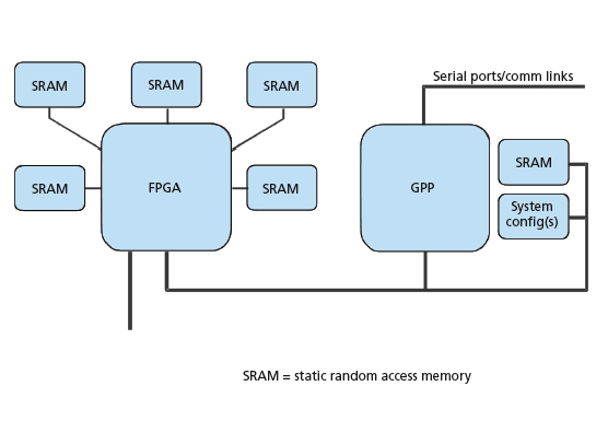
FPGAs are well suited to the development of deeply pipelined datapath applications typical in signal processing, while GPPs are better suited to system control and communication applications. This commonality in processing requirements led to the development of the Common Architecture for Microsensors (CAµS), which consists of a data acquisition module, digital signal processing (DSP) module, and FPGA module. CAµS is independent of a specific I/O technology and provides a large amount of user-defined digital I/O for interconnection to a variety of devices. The architecture can easily accommodate different radio technologies. The software and hardware can be programmed (configured) through a serial port with support to change the nonvolatile memory in situ. This nonvolatile memory is able to store four separate system configurations (DSP and FPGA configurations). Future work will provide the capability to remotely configure the system.
The system is partitioned into a sensor head, signal conditioning and processing, communication, and battery. An obvious system configuration is to integrate the processing, communication, and battery into a base unit, and the user could then attach sensor heads as needed for the application. Such a system could even act as a gateway for or a manager of a distributed sensor network. The system is based on a commercially available DSP and FPGA in a standard PC-104 form factor (4 × 4" stackable cards). The system consists of either four or five cards: the DSP card, a power card, a data acquisition card, and one or two FPGA cards, depending on the application.
The FPGA module consists of an FPGA and five static RAM memories of 256 k × 36 bits each. Connections between the FPGA and the other boards allow the FPGA to control the data acquisition module and to interrupt the DSP. Additionally, the FPGA is connected to the DSP bus, making it possible to memory- map FPGA resources into the DSP address space.
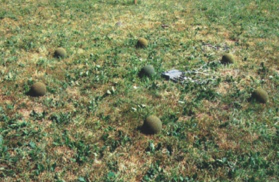
The first CAµS application developed was an acoustic sensor system for ground-vehicle detection and bearing estimation (Figure 2). The sensor array is formed by a collection of omnidirectional microphones, each providing 360° field-of-view coverage. The sensors are placed on or near the ground in a geometric shape to conform the array. The microphone array consists of seven microphones, six in an 8-foot-diameter circle and one in the center. The signals received at each of the microphones are sampled at 1 kHz and the resulting data are multiplied by a windowing function. After a corner turn of the data, seven 1,024-point Fast Fourier Transforms (FFTs) are performed.
A detection algorithm is then run on the FFT output magnitudes to identify possible targets. This is done in two stages. First, a peak picking algorithm estimates the noise floor and high-power frequency bins are selected with a threshold determined from that noise floor. Harmonic line analysis is performed to find groups of frequency bins that form a harmonic relationship. Groups containing enough frequency components are declared to be targets. In the second stage, beamforming is performed on the raw data at the target’s frequencies to determine exact target bearings. Finally, a tracking filter is applied to reduce the number of false reports and provide a lock on the target’s bearing, providing lines-of-bearing (LOB) updates once every second. This entire computation could be done on either the CAµS DSP or the CAµS FPGA alone.
Future work will focus on adapting CAµS for use with additional sensors and on miniaturizing the CAµS architecture. In this future microsensor system, the FPGA-based processor will be capable of supporting magnetic, acoustic, seismic, and imaging (day or infrared) sensors all in the same package. The FPGA will have to be reconfigured in real time to facilitate such a sensor suite.
This work was done by Mark Falco of Sanders and Andree Filipov of the Army Research Laboratory.
ARL-0036
This Brief includes a Technical Support Package (TSP).
Applying Reconfigurable Computing to Acoustic Sensors Using FPGAs
(reference ARL-0036) is currently available for download from the TSP library.
Don't have an account?
More From SAE Media Group
Aerospace & Defense Tech Briefs
Applying Reconfigurable Computing to Acoustic Sensors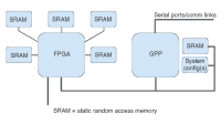
Medical Design Briefs
FPGA Technology for High-Speed Medical Image Processing
Aerospace & Defense Tech Briefs
Content Addressable Memory (CAM) Technologies for Big Data and Intelligent Electronics Enabled By Magneto-Electric Ternary CAM
Aerospace & Defense Tech Briefs
FPGAs and HPC
Automotive Engineering
Real-Time Processors Key to the Zonal E/E Revolution
Aerospace & Defense Tech Briefs
Designing for Compressive Sensing: Compressive Art, Camouflage, Fonts, and Quick Response Codes
Photonics & Imaging Technology
Rethinking FPGAs for Smart Cameras
Sensor Technology
Sensors Expo Preview 2019
Autonomous Vehicle Engineering
Daimler-Xilinx Linkup Spotlights Growing Use of FPGAs
Tech Briefs
Flexible Silicon-on-Polymer Chip
Aerospace & Defense Tech Briefs
Implementing On-Board Cloud Detection on a Reconfigurable Computer
Aerospace & Defense Tech Briefs
EW: New Challenges, Technologies, and Requirements
Aerospace & Defense Tech Briefs
A Focal Plane Array and Electronics Model for CMOS and CCD Sensors in the AFIT Sensor and Scene Emulation Tool
Aerospace & Defense Tech Briefs
Migrating Advanced Signal Processing Technology to Rugged SFF Platforms

Embedded Technology
Understanding Virtex FPGAs
Embedded Technology
Beamforming System Eases Crowded Wireless Spectrum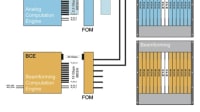
Aerospace & Defense Tech Briefs
Protecting Critical Data on Unmanned Underwater Platforms
Embedded Technology
Designing Versatile COTS Data Acquisition Systems
Tech Briefs
Crew Activity Analyzer
Aerospace INSIDER
TEWS Introduces First VITA 93 QMC Modules
Tech Briefs
RFID-Based System Enables Internet of Things
Tech Briefs
5 Ws of the Winged Flying Microchip
Aerospace & Defense Tech Briefs
Real-Time Simulation and Semiautomated Design of Complex ICs
Off-Highway Engineering
Shifting Design of Autonomous Architectures
Electronics & Sensors INSIDER
A New Neuromorphic Chip for AI on The Edge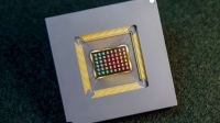
Tech Briefs
Four-Channel PC/104 MIL-STD-1553 Circuit Board
Tech Briefs
Wireless, Wearable Transmitter
Overview
The document titled "Application of Reconfigurable Computing to Acoustic Sensors" discusses the integration of digital signal processors (DSPs) and field-programmable gate arrays (FPGAs) in the development of advanced microsensor systems, particularly for military applications such as reconnaissance, surveillance, and target acquisition. The U.S. Army Research Laboratory and Sanders collaborated on this project, focusing on creating systems that are compact, lightweight, cost-effective, and capable of long operational lifespans.
Microsensors are designed to autonomously detect, classify, and localize targets in various environments, utilizing different sensor types (acoustic, seismic, magnetic, and imaging) to provide complementary data. A key challenge in these systems is managing power consumption, as communication bandwidth is often limited by power constraints. The document emphasizes that effective signal processing must occur within the microsensor to minimize data transmission and maximize information retention, which is crucial for maintaining stealth in sensitive operations.
The paper highlights the advantages of using FPGAs in conjunction with DSPs. While traditional DSPs like the Motorola 56307 consume significant power (up to 1500 mW at high frequencies), the Xilinx XCV1000 FPGA offers a quiescent power of 200 mW, with additional power consumption dependent on design complexity and operational frequency. The combination of these technologies allows for enhanced computational performance while significantly reducing overall power usage.
The document outlines a proof-of-concept system that integrates these components into a modular architecture, allowing for flexible configurations based on specific application needs. The FPGA module can control data acquisition and interact with the DSP, facilitating efficient data processing and communication.
Future work is suggested to explore the full range of scenarios where this hybrid approach can be applied, particularly in high-demand processing situations like beamforming across large sensor arrays. The potential for low-power FPGAs to revolutionize microsensor applications is underscored, with ongoing research aimed at further minimizing power consumption and enhancing computational capabilities.
In conclusion, the document presents a compelling case for the use of reconfigurable computing in microsensor systems, highlighting its benefits in power efficiency, flexibility, and performance, which are essential for modern military operations and beyond.
Top Stories
NewsRF & Microwave Electronics
![]() Microvision Aquires Luminar, Plans Relationship Restoration, Multi-industry Push
Microvision Aquires Luminar, Plans Relationship Restoration, Multi-industry Push
INSIDERAerospace
![]() A Next Generation Helmet System for Navy Pilots
A Next Generation Helmet System for Navy Pilots
INSIDERDesign
![]() New Raytheon and Lockheed Martin Agreements Expand Missile Defense Production
New Raytheon and Lockheed Martin Agreements Expand Missile Defense Production
INSIDERMaterials
![]() How Airbus is Using w-DED to 3D Print Larger Titanium Airplane Parts
How Airbus is Using w-DED to 3D Print Larger Titanium Airplane Parts
NewsPower
![]() Ford Announces 48-Volt Architecture for Future Electric Truck
Ford Announces 48-Volt Architecture for Future Electric Truck
ArticlesAR/AI
Webcasts
Electronics & Computers
![]() Cooling a New Generation of Aerospace and Defense Embedded...
Cooling a New Generation of Aerospace and Defense Embedded...
Automotive
![]() Battery Abuse Testing: Pushing to Failure
Battery Abuse Testing: Pushing to Failure
Power
![]() A FREE Two-Day Event Dedicated to Connected Mobility
A FREE Two-Day Event Dedicated to Connected Mobility
Unmanned Systems
![]() Quiet, Please: NVH Improvement Opportunities in the Early Design Cycle
Quiet, Please: NVH Improvement Opportunities in the Early Design Cycle
Automotive
![]() Advantages of Smart Power Distribution Unit Design for Automotive &...
Advantages of Smart Power Distribution Unit Design for Automotive &...
Energy
![]() Sesame Solar's Nanogrid Tech Promises Major Gains in Drone Endurance
Sesame Solar's Nanogrid Tech Promises Major Gains in Drone Endurance