


Graphene Advances May Lead to Improved Data Transmission, Storage

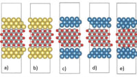
The phenomenon known as "spin filtering" is due to an interaction of the quantum mechanical properties of graphene with those of a crystalline nickel film. When the nickel and graphene structures align, only electrons with one spin can pass easily from one material to the other, or spin filtering, that results in spin polarization of an electric current.
The U.S. Naval Research Laboratory (NRL) took advantage of an interdisciplinary team of scientists to successfully demonstrate metallic spin filtering at room temperature using ferromagnet-graphene-ferromagnet thin film junction devices. Spin is said to be a fundamental property of electrons, in addition to charge, that can be used to transmit, process, and store data; and room temperature is said to be the breakthrough that may lead to the technology's more commonplace use.
“Spin filtering had been theoretically predicted and previously seen only for high-resistance structures at cryogenic temperatures,” said Dr. Enrique Cobas, Principal Investigator, NRL Materials Science and Technology Division. “The new results confirm the effect works at room temperature with very low resistance in arrays of multiple devices.”
The thin film junctions demonstrated low resistance, and the magnetoresistance characteristic of a spin filter interface from cryogenic temperatures to room temperature. The research team also developed a device model to incorporate the predicted spin filtering by explicitly treating a metallic minority spin channel with spin current conversion, and determined that the spin polarization was at least 80% in the graphene layer.
“Graphene is famous for its extraordinary in-plane properties, but we wanted to look at conductivity between stacked graphene sheets and how they interact with other materials,” said Cobas.
To do so, NRL researchers developed a method to grow large multi-layer graphene films directly on a smooth, crystalline nickel alloy film while retaining that film’s magnetic properties, then patterned the film into arrays of cross-bar junctions.
“We also wanted to show we could produce these devices with standard industry tools, not just make one device,” Cobas added.
According to Dr. Olaf van't Erve, a research scientist at NRL Materials Science and Technology Division, there is room for improvement as theory suggests the effect can be increased by an order of magnitude by fine-tuning the number of graphene layers.
“However, current models do not include the spin-conversion that happens inside the ferromagnetic contacts," he said. " Once we account for those effects, we’re already close to the ideal case of 100% spin polarization in the graphene layer, enabling us to revise our device geometry and materials to maximize the effect.”
The result is relevant to next-generation non-volatile magnetic random access memory (MRAM), which uses spin-polarized pulses to flip a magnetic bit from 0 to 1 and vice-versa. It may also find use in future spin logic technologies or as magnetic sensors.
More From SAE Media Group

Aerospace & Defense Tech Briefs
Ensuring Aircraft Safety Requires Right Wheel Inspection Equipment
Aerospace & Defense Tech Briefs
Fiber Laser Sensor Technology for Structural Health Monitoring
Aerospace & Defense Tech Briefs
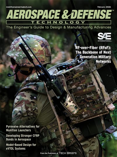
Heat-Pipe Embedded CFRP Enclosures for Electronics Thermal Management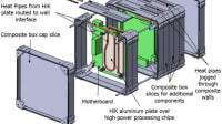

Aerospace & Defense Tech Briefs
3D Scanning Provides Key Weapon for Aerospace and Defense Manufacturing
Defense INSIDER
NRL Develops Novel Monolayer Ferroelectric Hybrid Structures
Aerospace & Defense Tech Briefs
Advances in Adhesive Joining of Structural Components Focus of New Book from SAE International
Aerospace & Defense Tech Briefs
Altair Optimizes 3D-Printed Structures for Complex, Lightweight Designs

Aerospace Manufacturing and Machining
Lightweighting Parts Using 3D Metal Printing
Electronics & Sensors INSIDER
Blocking Electromagnetic Radiation with the Flip of a Switch
Aerospace & Defense Tech Briefs
CAD-CAM-CNC System
Aerospace & Defense Tech Briefs
Physics-Guided Neural Network for Regularization and Learning Unbalanced Data Sets
Defense INSIDER
Air Force Scientists Discover Unique Stretchable Conductor


Defense INSIDER
Scientists Print Radio Frequency Antenna with Graphene Ink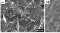
Defense INSIDER
NRL Researchers’ Golden Touch Enhances Quantum Technology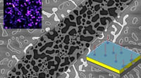
Photonics & Imaging Technology INSIDER
Optics Breakthrough Could Revamp Night Vision
Aerospace & Defense Tech Briefs
Nanotechnology May Lead to Huge Advances in Engines of the Future
Aerospace & Defense Tech Briefs
Cold Spray Technology
Aerospace & Defense Tech Briefs
High-Performance Enclosure Systems for Aerospace and Defense Applications: Preparing for What’s Next
Defense INSIDER
Navy Scientists Discover New Class of Semiconductor Nanocrystals
Robotics & Automation INSIDER
New Imaging Technique Reconstructs the Shapes of Hidden Objects
Aerospace & Defense Tech Briefs
Surviving the Challenge of Thermal Design in Aerospace Electronics
Aerospace & Defense Tech Briefs
Coating Technology Enables Effective Missile Countermeasures

Top Stories
INSIDERDefense
![]() New Raytheon and Lockheed Martin Agreements Expand Missile Defense Production
New Raytheon and Lockheed Martin Agreements Expand Missile Defense Production
NewsAutomotive
![]() Ford Announces 48-Volt Architecture for Future Electric Truck
Ford Announces 48-Volt Architecture for Future Electric Truck
INSIDERManufacturing & Prototyping
![]() Active Strake System Cuts Cruise Drag, Boosts Flight Efficiency
Active Strake System Cuts Cruise Drag, Boosts Flight Efficiency
ArticlesTransportation
![]() Accelerating Down the Road to Autonomy
Accelerating Down the Road to Autonomy
INSIDERMaterials
![]() How Airbus is Using w-DED to 3D Print Larger Titanium Airplane Parts
How Airbus is Using w-DED to 3D Print Larger Titanium Airplane Parts
Road ReadyTransportation
Webcasts
Electronics & Computers
![]() Cooling a New Generation of Aerospace and Defense Embedded...
Cooling a New Generation of Aerospace and Defense Embedded...
Power
![]() Battery Abuse Testing: Pushing to Failure
Battery Abuse Testing: Pushing to Failure
Connectivity
![]() A FREE Two-Day Event Dedicated to Connected Mobility
A FREE Two-Day Event Dedicated to Connected Mobility
Automotive
![]() Quiet, Please: NVH Improvement Opportunities in the Early Design Cycle
Quiet, Please: NVH Improvement Opportunities in the Early Design Cycle
Transportation
![]() Advantages of Smart Power Distribution Unit Design for Automotive &...
Advantages of Smart Power Distribution Unit Design for Automotive &...
Aerospace
![]() Sesame Solar's Nanogrid Tech Promises Major Gains in Drone Endurance
Sesame Solar's Nanogrid Tech Promises Major Gains in Drone Endurance