


GE Scanner Enhances Defect Detection for Industrial CT
GE Measurement & Control is offering its proprietary scatter|correct technology to industrial microCT users of GE’s phoenix v|tome|x m CT (computed tomography) system. It provides CT data quality improvements for high energy microfocus CT scans with up to 300 kV.
The scatter|correct technology enhances defect detection and analysis as well as 3D metrology in mobility sectors including aerospace, automotive, and off-highway, as well as the power generation industry. It can be applied to high scattering materials such as steel and aluminum, composites, and multi-material samples.
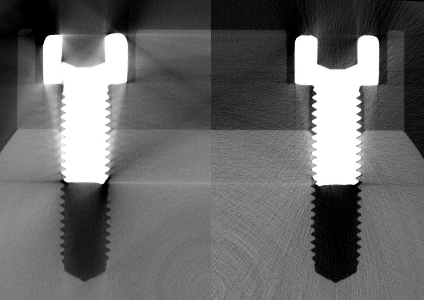
The main improvement offered by scatter|correct, a company spokesman told SAE Magazines, is that “it really measures and removes scatter, not simulates scatter based on sample material and geometry estimations.” He added that it can be applied to large light-metal castings with a diameter up to 600 mm (23.6 in) or small higher absorbing steel components such as injection nozzles.
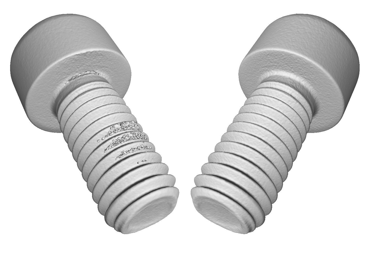
GE’s scatter|correct technology, featuring both hardware and software advances, automatically removes scatter artifacts from the CT volume, allowing users to gain a low scatter artifact quality level “never before reached” with conventional cone beam microCT, the company claims. Process control productivity on the production floor is reportedly increased by improved quantitative volume evaluations, such as automatic defect recognition (ADR) or more precise 3D metrology results.
“GE’s breakthrough scatter|correct innovation really changes the limitations of industrial CT. Until now, CT manufacturers had to increase the X-ray energies to minimize the negative scatter radiation quality impact,” Dr. Oliver Brunke, Senior CT Product Manager at GE Measurement & Control, said in a statement. “But this led to more complex, heavier shielded and expensive systems. With scatter|correct, CT users can now perform in many cases scans normally requiring a 450 kV X-ray tube with a 300 kV X-ray tube by using the available tube spectrum much more effectively.”
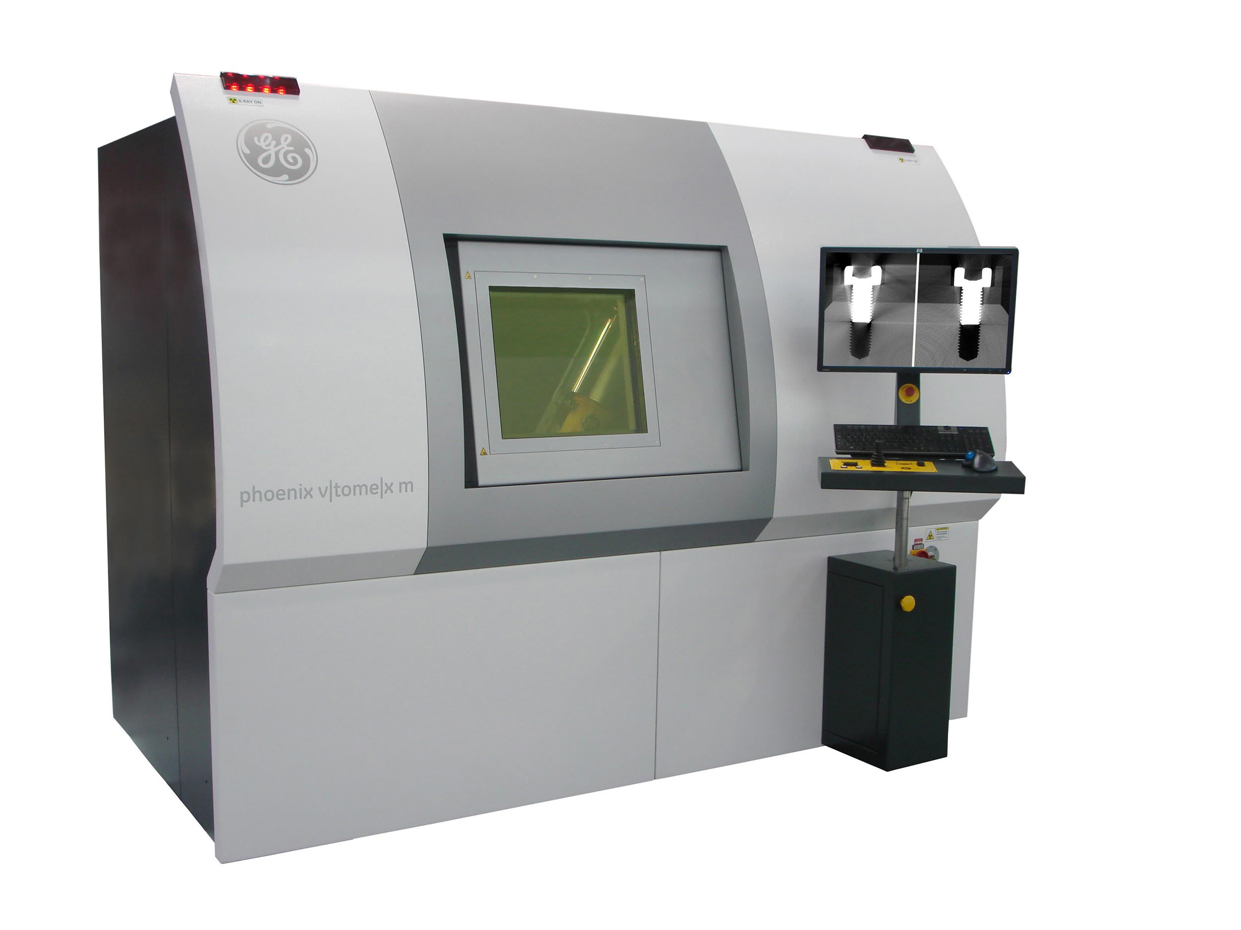
The phoenix v|tome|x m is an X-ray microfocus CT system with optional high resolution nanoCT capability for 3D metrology and failure analysis with up to 300 kV/500 W. With <1 µm detail detectability, the system offers what GE claims is industry-leading magnification and power at 300 kV. GE’s click & measure|CT acquisition, reconstruction and evaluation automation functionality adds to the efficiency and reproducibility of the 3D evaluation tool.
The phoenix v|tome|x m system is also available as a metrology edition. The optional dual tube configuration enables high resolution nanoCT of low absorbing samples, which makes the new system suitable for a range of applications in the materials-science area as well.
More From SAE Media Group


Test & Measurement Tech Briefs
Computed Tomography Systems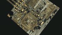
Aerospace & Defense Tech Briefs
Robotic Rotational Molding Creates New Opportunities for Military and Aerospace Applications

Aerospace & Defense Tech Briefs
Designing for Space and Other Extreme Environments
Aerospace & Defense Tech Briefs
A Secure Attachment to 3D Printing
Medical Manufacturing and Machining
New Products & Services
Aerospace & Defense Tech Briefs
X-Ray Testing for Large Composites

Tech Briefs
Rising Star Awards 2025 Judges


Tech Briefs
2025 Award Finalists


Off-Highway Engineering
Noncontact Laser Scanner
Tech Briefs
Versatile 3D Machine Vision Technology
Aerospace & Defense Tech Briefs
3D Printing Metal Parts on a Ship
Tech Briefs
Optimizing a CubeSat with Architected Materials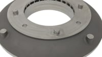
Tech Briefs
Liquid Security Screening Technology

Defense INSIDER
Northrop Grumman Assembles First Manta Ray UUV Prototype

Defense INSIDER
Using Squeezed Light to Develop Sensors That Defy Defense Limits
Tech Briefs
RISING STAR AWARDS 2025 WINNERS ANNOUNCEDTop Stories
INSIDERManufacturing & Prototyping
![]() How Airbus is Using w-DED to 3D Print Larger Titanium Airplane Parts
How Airbus is Using w-DED to 3D Print Larger Titanium Airplane Parts
INSIDERManned Systems
![]() FAA to Replace Aging Network of Ground-Based Radars
FAA to Replace Aging Network of Ground-Based Radars
NewsTransportation
![]() CES 2026: Bosch is Ready to Bring AI to Your (Likely ICE-powered) Vehicle
CES 2026: Bosch is Ready to Bring AI to Your (Likely ICE-powered) Vehicle
NewsSoftware
![]() Accelerating Down the Road to Autonomy
Accelerating Down the Road to Autonomy
EditorialDesign
![]() DarkSky One Wants to Make the World a Darker Place
DarkSky One Wants to Make the World a Darker Place
INSIDERMaterials
![]() Can This Self-Healing Composite Make Airplane and Spacecraft Components Last...
Can This Self-Healing Composite Make Airplane and Spacecraft Components Last...
Webcasts
Defense
![]() How Sift's Unified Observability Platform Accelerates Drone Innovation
How Sift's Unified Observability Platform Accelerates Drone Innovation
Automotive
![]() E/E Architecture Redefined: Building Smarter, Safer, and Scalable...
E/E Architecture Redefined: Building Smarter, Safer, and Scalable...
Power
![]() Hydrogen Engines Are Heating Up for Heavy Duty
Hydrogen Engines Are Heating Up for Heavy Duty
Electronics & Computers
![]() Advantages of Smart Power Distribution Unit Design for Automotive...
Advantages of Smart Power Distribution Unit Design for Automotive...
Unmanned Systems
![]() Quiet, Please: NVH Improvement Opportunities in the Early Design...
Quiet, Please: NVH Improvement Opportunities in the Early Design...