


Researchers Developing Prototype of Next-Gen Night Vision Technology
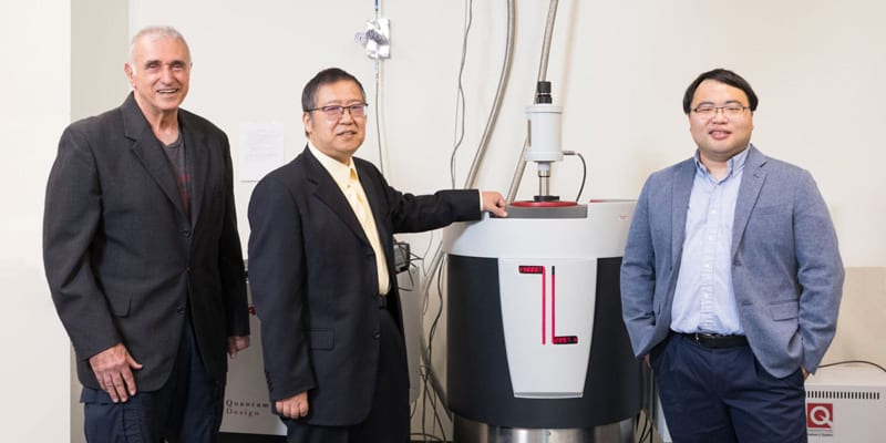
Three University of Arkansas researchers — electrical engineering professor Shui-Qing “Fisher” Yu, Distinguished Professor Greg Salamo, and Jin Hu, assistant professor of physics — will collaborate with the Navy Surface Warfare Research Center, Crane Division, and local company Arktonics to use the semiconductor silicon germanium tin in designing and building a prototype of a superior and less-expensive infrared camera. The military uses infrared imaging technologies for night vision technology.
A $4.4 million grant from the U.S. Office of Naval Research will pay for specially designed equipment that will help the team develop the infrared imaging sensor array made of silicon germanium tin. The team will then integrate this array with a complementary metal oxide semiconductor (CMOS) on the same chip. CMOS technology is used for making integrated-circuit chips for microprocessors, controllers and other digital and analog circuits, including image sensors. The combination is more effective at harnessing ambient light, an essential element in night vision technology.
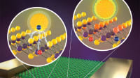
Current technologies rely on semiconducting alloys such as mercury cadmium telluride and other material-based photodetectors. These alloys have several limitations, including a complex and expensive manufacturing process, low production yield, and poor uniformity over large areas. These limitations negatively affect wide-range infrared visibility, especially in areas with poor environmental conditions, such as sandy or hazy environments. These technologies also cannot integrate an infrared camera and other necessary electronics on the same chip, which increases cost and decreases reliability, efficiency, and speed.
By more efficiently harnessing light, silicon germanium tin on silicon substrates is potentially a better solution. Yu has worked with silicon germanium tin for more than a decade. In 2016, he and colleagues reported the fabrication of a first-generation, “optically pumped” laser, meaning the material was injected with light, similar to an injection of electrical current. Yu was also the first to report an “electrical excited” germanium tin laser.
Using molecular beam epitaxy, Salamo has been growing semiconductor nanostructures for more than 20 years. He is well known for his work on quantum wells, dots and wires. Meanwhile, Hu has developed and fabricated new quantum materials and investigated their novel quantum properties.
More From SAE Media Group
Tech Briefs
High-Efficiency Laser for Silicon Chips
Aerospace & Defense Tech Briefs
New Diamond Super-Material Enhances Aircraft Survivability
Electronics & Sensors INSIDER
MIT Engineers Grow “High-Rise” 3D Chips
Photonics & Imaging Technology
Multicolored Light-Emitting Array on a Single Chip
Tech Briefs
A More Responsive Infrared Photodiode

Electronics & Sensors INSIDER
Engineers “Grow” Atomically Thin Transistors on Top of Computer Chips
Photonics & Imaging Technology
Optimizing Laser Cutting in Semiconductor Advanced Packaging
Photonics & Imaging Technology INSIDER
Miniaturized Infrared Detectors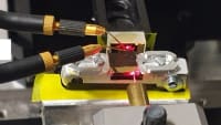
Electronics & Sensors INSIDER
A New Kind of Transistor — A Conductive Polymer
Aerospace & Defense Tech Briefs
Future Advances in Electronic Materials and Processes - Flexible Hybrid Electronics
Photonics & Imaging Technology INSIDER
European Defense Fund Project to Produce Strategic Electronics for Next Generation Infrared Sensors
Electronics & Sensors INSIDER
Scientists Create Superconducting Semiconductor Material

Tech Briefs
Chip Measures Quantities with Quantum Precision

Tech Briefs
Turning Diamond into Metal
Photonics & Imaging Technology
Material Advances for LED Quantum Dot Efficiency
Electronics & Sensors INSIDER
MIT Team Takes a Major Step Toward Fully 3D-Printed Active Electronics
Tech Briefs
5Ws of the Silk Transistor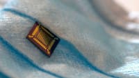
Electronics & Sensors INSIDER
This Advance May Enable 2D Transistors for Tinier Microchip Components

Electronics & Sensors INSIDER
Manufacturing the World's Tiniest Light-Emitting Diodes
Photonics & Imaging Technology INSIDER
Light from Exotic Crystal Semiconductor Could Lead to Better Solar Cells

Electronics & Sensors INSIDER
2D Materials for Extra Thin Computer Chips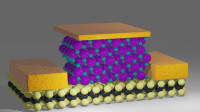
Tech Briefs
Combined Optical Transmitter and Receiver
Aerospace & Defense Tech Briefs
New 3D Chips Could Make Electronics Faster and More Energy-Efficient
Top Stories
NewsSensors/Data Acquisition
![]() Microvision Aquires Luminar, Plans Relationship Restoration, Multi-industry Push
Microvision Aquires Luminar, Plans Relationship Restoration, Multi-industry Push
INSIDERRF & Microwave Electronics
![]() A Next Generation Helmet System for Navy Pilots
A Next Generation Helmet System for Navy Pilots
INSIDERWeapons Systems
![]() New Raytheon and Lockheed Martin Agreements Expand Missile Defense Production
New Raytheon and Lockheed Martin Agreements Expand Missile Defense Production
NewsAutomotive
![]() Ford Announces 48-Volt Architecture for Future Electric Truck
Ford Announces 48-Volt Architecture for Future Electric Truck
INSIDERAerospace
![]() Active Strake System Cuts Cruise Drag, Boosts Flight Efficiency
Active Strake System Cuts Cruise Drag, Boosts Flight Efficiency
ArticlesTransportation
Webcasts
Aerospace
![]() Cooling a New Generation of Aerospace and Defense Embedded...
Cooling a New Generation of Aerospace and Defense Embedded...
Energy
![]() Battery Abuse Testing: Pushing to Failure
Battery Abuse Testing: Pushing to Failure
Power
![]() A FREE Two-Day Event Dedicated to Connected Mobility
A FREE Two-Day Event Dedicated to Connected Mobility
Automotive
![]() Quiet, Please: NVH Improvement Opportunities in the Early Design Cycle
Quiet, Please: NVH Improvement Opportunities in the Early Design Cycle
Electronics & Computers
![]() Advantages of Smart Power Distribution Unit Design for Automotive &...
Advantages of Smart Power Distribution Unit Design for Automotive &...
Unmanned Systems
![]() Sesame Solar's Nanogrid Tech Promises Major Gains in Drone Endurance
Sesame Solar's Nanogrid Tech Promises Major Gains in Drone Endurance