Stencil Mask Methodology for Parallelized Production of Microscale Mechanical Test Samples
This methodology parallelizes the production of micromechanical test samples from bulk materials.
Over the past decade, there has been considerable progress in the development of new mechanical testing methods to characterize the properties of materials at the micro and nano scales. One common application of these testing methodologies is the measurement of mechanical properties of structures that are physically small in scale, such as the strength of nanowhiskers and MEMS devices. Another common application is the use of small sample testing to gain insight into plastic deformation processes through systematic alteration of the sample dimensions in order to help isolate selected aspects of material behavior. Examples of these studies include the exploration of size-scale strengthening effects, the quantitative measurement and analysis of dislocation avalanches, and the measurement of local property variations in engineering alloys.

The present work describes a new sample preparation methodology, using ion beam sputtering for material removal, which provides a parallelized production process to enable statistical measurements of microscale mechanical properties. The methodology is inspired by an ion sputtering process termed slope-cutting, which uses a physical mask with a well-defined edge, such as a knifeedge blade used for machine tooling, and a broad ion beam source to prepare a cross-section surface. The physical mask protects one portion of the sample while the edge defines the location of a cross-section surface that is created when the remainder of the sample is eroded by the ion beam. Slope-cutting maintains some of the advantages of FIB cross-section preparation, such as the ability to cleanly section multiphase materials while retaining features such as porosity, and the ability to apply the method to a wide variety of materials. Yet the dramatic increase in total ion current from 50 nA to hundreds of A or higher results in a much shorter time to sputter mesoscopic volumes of material. In addition, the equipment used to perform a slope-cutting experiment is simpler and usually much less expensive than a FIB microscope.
Instead of using a simple rectilinear mask as in slope cutting, the methodology uses microelectronics processing techniques to create physical masks with complex twodimensional shapes, i.e. stencil masks. The stencil mask methodology consists of three primary tasks. The first task is to create a freestanding stencil mask, which defines the pattern that is to be transferred to the substrate. The second step is to ensure that the substrate is in a suitable form for creating a threedimensional test sample via ion sputtering, where the region of interest is a thinned section with uniform thickness on the order of 20 to 100 μm. The final step is to use the stencil mask in conjunction with broad ion beam milling to transfer the pattern into the substrate.
Compared with conventional FIBbased fabrication, the methodology provides a fast and relatively low-cost processing route to manufacture an array of test structures with dimensions that range from 20 to 200 μm in scale. The methodology has been successfully demonstrated using stencil masks made from Si wafers, and pattern transfer to a Ni foil was demonstrated using a commercial broad ion beam milling system.
This work was done by Paul A. Shade and Michael D. Uchic of the Air Force Research Laboratory, and Sang-Lan Kim and Robert Wheeler of UES, Inc. AFRL-0221
This Brief includes a Technical Support Package (TSP).
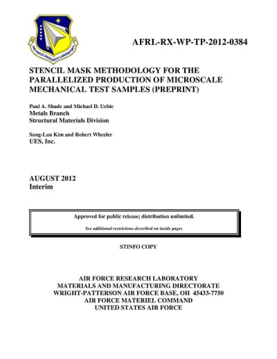
Stencil Mask Methodology for Parallelized Production of Microscale Mechanical Test Samples
(reference AFRL-0221) is currently available for download from the TSP library.
Don't have an account?
Overview
The document titled "Stencil Mask Methodology for the Parallelized Production of Microscale Mechanical Test Samples" presents a novel approach to efficiently fabricate micromechanical test samples from bulk materials. Authored by Paul A. Shade, Michael D. Uchic, Sang-Lan Kim, and Robert Wheeler, the paper outlines a methodology aimed at reducing the unit cost per sample compared to traditional focused ion beam (FIB) fabrication techniques.
The proposed method utilizes standard microelectronic processes, including photolithography and deep-reactive ion etching (DRIE), to create high aspect ratio patterned templates known as stencil masks from silicon wafers. These stencil masks are designed to produce tensile samples with dimensions typically ranging from 20 to 200 micrometers. The innovative aspect of this methodology is the parallelization of the sample production process, which allows for the simultaneous fabrication of multiple samples, thereby increasing efficiency.
Once the stencil mask is prepared, it is placed on a pre-thinned substrate. The mask and substrate are then co-sputtered using a broad ion beam milling system, specifically a Gatan Precision Etching and Coating System (PECS). This system employs low-energy argon ions to sputter both the mask and substrate, effectively transferring the mask pattern into the substrate material. The document emphasizes the importance of understanding the relative sputter erosion rates of the mask and substrate materials, as this affects the design and effectiveness of the stencil mask.
The methodology is demonstrated through the fabrication of an array of metallic micro-tension samples using a silicon stencil mask and a polycrystalline nickel foil. The results indicate that this approach not only streamlines the production process but also enhances the precision and reproducibility of the samples produced.
In summary, this technical paper provides a comprehensive overview of a new stencil mask methodology that leverages established microfabrication techniques to produce microscale mechanical test samples more efficiently and cost-effectively. The findings have significant implications for the fields of materials science and engineering, particularly in the development of micromechanical devices and testing methodologies. The research was conducted at the Air Force Research Laboratory and is approved for public release, ensuring that the insights gained can benefit a wider audience.
Top Stories
INSIDERManufacturing & Prototyping
![]() How Airbus is Using w-DED to 3D Print Larger Titanium Airplane Parts
How Airbus is Using w-DED to 3D Print Larger Titanium Airplane Parts
INSIDERManned Systems
![]() FAA to Replace Aging Network of Ground-Based Radars
FAA to Replace Aging Network of Ground-Based Radars
NewsTransportation
![]() CES 2026: Bosch is Ready to Bring AI to Your (Likely ICE-powered) Vehicle
CES 2026: Bosch is Ready to Bring AI to Your (Likely ICE-powered) Vehicle
NewsSoftware
![]() Accelerating Down the Road to Autonomy
Accelerating Down the Road to Autonomy
EditorialDesign
![]() DarkSky One Wants to Make the World a Darker Place
DarkSky One Wants to Make the World a Darker Place
INSIDERMaterials
![]() Can This Self-Healing Composite Make Airplane and Spacecraft Components Last...
Can This Self-Healing Composite Make Airplane and Spacecraft Components Last...
Webcasts
Defense
![]() How Sift's Unified Observability Platform Accelerates Drone Innovation
How Sift's Unified Observability Platform Accelerates Drone Innovation
Automotive
![]() E/E Architecture Redefined: Building Smarter, Safer, and Scalable...
E/E Architecture Redefined: Building Smarter, Safer, and Scalable...
Power
![]() Hydrogen Engines Are Heating Up for Heavy Duty
Hydrogen Engines Are Heating Up for Heavy Duty
Electronics & Computers
![]() Advantages of Smart Power Distribution Unit Design for Automotive...
Advantages of Smart Power Distribution Unit Design for Automotive...
Unmanned Systems
![]() Quiet, Please: NVH Improvement Opportunities in the Early Design...
Quiet, Please: NVH Improvement Opportunities in the Early Design...


