


Micromachining and Material Processing with Amplified Picosecond Lasers
Short pulsed lasers are presently an important tool for manufacturing a variety of devices from smart phones to photovoltaics. When wielded correctly, these lasers can remove material with far greater precision than mechanical tools or more conventional laser processing using CW or pulsed Qswitched lasers. New developments in the design of picosecond laser amplifiers have resulted in improved durability, maintainability, and lower costs.
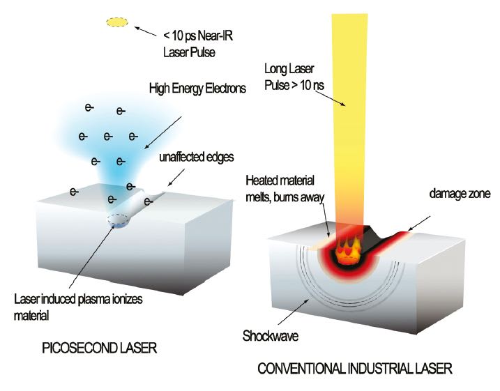
In the world of laser fabrication, nanosecond and Q-Switched lasers have limitations because they cannot efficiently cut transparent material and often suffer from bad edge cut quality and surface roughness. With far shorter pulses, picosecond lasers are capable of better cut quality and can produce structures that conventional lasers cannot. They are considered universal tools in microfabrication as they are less sensitive to the properties of the materials and can even cut transparent material. When wielded properly, picosecond lasers can remove material with extreme precision due to an ablation mechanism with negligible thermal and mechanical stress. This ablation mechanism is precise enough to selectively remove extremely thin layers (10-100nm) without disturbing the underlying material. Picosecond laser micromachining now enables new methods for manufacturers to produce structures comparable to traditional semiconductor lithographic masks, but without the masks or dangerous chemicals, and in essentially any material that is desired.
Cold Ablation/Multiphoton Ionization


Glass
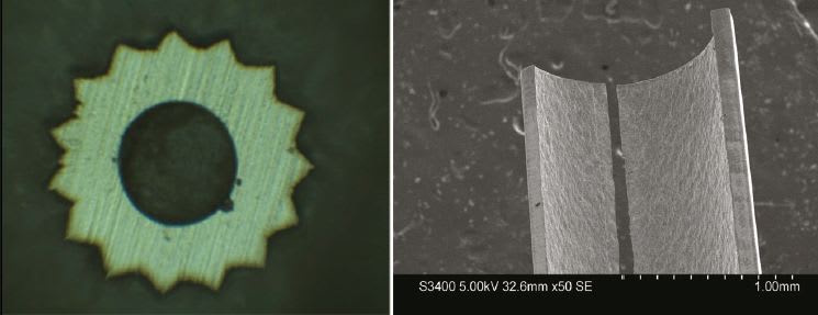
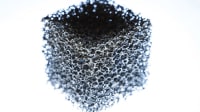
Microscopic features in glass, sapphire, and other transparent materials are easily achieved with picosecond micromachining. Material removal rates in glass can vary from ~0.1 to >1 mm3/min*W for optimized processes. The microfluidic mixer structures of Figure 3 are milled from one side. The fluid can travel from one 20-um diameter entrance hole, along the branches and into the mixing chamber. Burrs are not allowed in micrfluidic microstructures as they cause fluid flow obstruction.
Steel
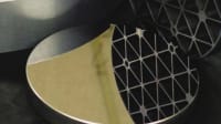
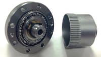
Numerous applications exist, particularly in the manufacturing of medical devices, in which stainless steel and other tough alloys must be micromachined without defects such as burrs. With picosecond lasers, material removal rates can be achieved ranging from 0.05 to 0.2mm3/min*W. Shown in Figure 4 is a micro gear produced for use in conjunction with a microfluidic mixer for secondary stage fluid mixing. Such tiny devices can be integrated into existing MEMS actuators. To ensure the smooth operation of these sensitive devices, the edge quality must be burr-free. Difficulty in fabrication of such pieces include handling and removal of debris from the cutting process. In this case, the only post-production procedure employed is the use of cleaning tissue to remove debris generated from cutting. Existing microgears made from silicon often suffer from debris formation due to wear and tear over time. Stainless steel gears promise to be significantly more durable and can minimize or eliminate debris formation from wear and tear.
Silicon
During solar cell manufacturing, layers of conductive material are deposited on top of each other. To avoid electrically shorting the solar cell to itself, a thin scribe line is needed to electrically isolate the solar cell. While nanosecond lasers can perform this task, there is a very high risk for nanosecond lasers to form microcracks within the thin solar cell substrate. Sometimes the crack will not appear for years, but even that cannot be tolerated. Microcracks can completely change the electronic structure within the silicon crystal and may cause unwanted electrical insulation.
Crystalline solar cells are generally pseudo-squares. A silicon wafer is diced on 4 edges and the off-cuts of the solar grade pure silicon are recycled back into the melt pool. Traditionally, dicing is done using a diamond saw. Diamond saws wear out over time and both nanosecond lasers and diamond saws can cause undesired micro cracking, which leads to losses in solar cell efficiency and shorter cell lifetimes. Picosecond lasers can eliminate these microcracks while dicing at m/sec speeds.
Plastics

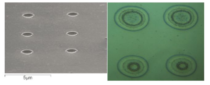
Of particular importance in manufacturing of thin film devices is the ability to remove insulating layers to expose microscopic circuitry for testing or repair. Transparent coatings such as ITO or conformal coatings pose an insurmountable problem for nanosecond lasers that either transmit through the coatings, damaging the layers underneath, or deposit heat that degrades underlying structures. Correct optimization of picosecond material removal can result in clean and complete layer removal, as shown in Figure 6.
The need for picosecond material processing is expected to grow by faster than 40% over the next few years and has been adopted as standard manufacturing practice by many well known firms. Attodyne currently produces commercially available picosecond laser systems for low to medium throughout applications such as repair of thin film transistors (TFT, used in flat panel displays such as TVs and laptops), repair of printed circuit boards and masks (used for the production of microchips), and also dicing, scribing and interconnecting wafers (e.g. for microchip and solar panel manufacturing).
This article was written by Darren Kraemer, President, and Dr. Michael Cowan, CEO, Attodyne Inc. (Toronto, Ontario, Canada). For more information, Click Here .
More From SAE Media Group
Aerospace & Defense Tech Briefs
Evaluation of Additively Manufactured Ultrahard Steels
Tech Briefs
5 Ws of Invisible Glass
Aerospace & Defense Tech Briefs
New Diamond Super-Material Enhances Aircraft Survivability
Tech Briefs
Method 3D-Prints Marine-Grade Stainless Steel
Aerospace & Defense Tech Briefs
Laser Integration on Silicon Photonic Circuits Through Transfer Printing
Aerospace & Defense Tech Briefs
Silicon Microsphere Fabrication

Tech Briefs
Products of Tomorrow
Aerospace & Defense Tech Briefs
Outsourcing Plasma Treatments for Surface Modification

Tech Briefs
Molten Target Sputtering (MTS) Deposition
Tech Briefs
Metallization for SiC Semiconductors
Aerospace & Defense Tech Briefs
Streamlining Post-Processing in Additive Manufacturing
Aerospace & Defense Tech Briefs
Improving Component Life in Abrasive, Corrosive Aerospace Environments
Photonics & Imaging Technology
Key Trends in Custom Optics for Aerospace


Aerospace & Defense Tech Briefs
Hydraulic Testing of Polymer Matrix Composite 102mm Tube Section
Aerospace & Defense Tech Briefs
The Science of Joining Dissimilar Metals in Aerospace Manufacturing
Tech Briefs
Generating Electrical Power from Waste Heat
Tech Briefs
Method Produces Fine-Grained Targets
Aerospace Manufacturing and Fabrication
New Products & Services
Aerospace & Defense Tech Briefs
More Bang for the Buck: A New Design and Manufacturing Method for Deep Penetrating Bomb Cases

Top Stories
INSIDERManufacturing & Prototyping
![]() How Airbus is Using w-DED to 3D Print Larger Titanium Airplane Parts
How Airbus is Using w-DED to 3D Print Larger Titanium Airplane Parts
INSIDERManned Systems
![]() FAA to Replace Aging Network of Ground-Based Radars
FAA to Replace Aging Network of Ground-Based Radars
NewsTransportation
![]() CES 2026: Bosch is Ready to Bring AI to Your (Likely ICE-powered) Vehicle
CES 2026: Bosch is Ready to Bring AI to Your (Likely ICE-powered) Vehicle
NewsSoftware
![]() Accelerating Down the Road to Autonomy
Accelerating Down the Road to Autonomy
EditorialDesign
![]() DarkSky One Wants to Make the World a Darker Place
DarkSky One Wants to Make the World a Darker Place
INSIDERMaterials
![]() Can This Self-Healing Composite Make Airplane and Spacecraft Components Last...
Can This Self-Healing Composite Make Airplane and Spacecraft Components Last...
Webcasts
Defense
![]() How Sift's Unified Observability Platform Accelerates Drone Innovation
How Sift's Unified Observability Platform Accelerates Drone Innovation
Automotive
![]() E/E Architecture Redefined: Building Smarter, Safer, and Scalable...
E/E Architecture Redefined: Building Smarter, Safer, and Scalable...
Power
![]() Hydrogen Engines Are Heating Up for Heavy Duty
Hydrogen Engines Are Heating Up for Heavy Duty
Electronics & Computers
![]() Advantages of Smart Power Distribution Unit Design for Automotive...
Advantages of Smart Power Distribution Unit Design for Automotive...
Unmanned Systems
![]() Quiet, Please: NVH Improvement Opportunities in the Early Design...
Quiet, Please: NVH Improvement Opportunities in the Early Design...