


Wide-Field Imaging System and Rapid Direction of Optical Zoom
This system demonstrates non-mechanical zoom using flexible thin films.
A breadboard system has been developed for demonstrating nonmechanical zoom using flexible thin films. The project consists of three major task areas: material characterization, diagnostic system development, and imaging system development. The material characterization phase involves two components: development of modeling tools, and measurement of material properties for use in the tools. The diagnostic system development phase will apply the tools and knowledge developed in the first phase to build algorithms for modeling and testing one-dimensional films with multiple actuators. These models will then be compared to experimental results and modified as needed. The imaging system development phase will conclude the effort by building a sensor system with variable zoom based on optical-quality PVDF films.
Modeling has focused on developing an empirical model for the film behavior and incorporating it into COMSOL. In the past, PVDF actuators were formed by combining two layers of materials that were poled with different orientations. The materials then act like a bimetallic strip used in a thermostat. Given the same field, one layer of the bimorph material would expand and one layer would contract, resulting in a curvature. This process is not amenable to opticalquality films because of the distortion created by attaching the two films.
A process was developed that generates a curvature from a unimorph film that can be fabricated with an opticalquality surface. The current focus is on actual material characterization. In the test fixture for characterizing the material properties, an upper bracket is used to connect the film to high voltage and hold it rigidly. A lower bracket is balanced on a knife edge, and will be used to connect the film to ground and apply a load to the film. There is a mirror mount on one end of the lower bracket. A laser will be reflected off this mount to measure deformations of the film as voltage is applied and the load is varied. Initial modeling using material constants for PVDF indicate a deformation of ~0.4% in length can be expected with 1 kV applied. For test samples with a 50-mm active area, that yields a deformation of 200 μm. This deformation will result in a 4-mrad deflection of the laser spot, or about 10× larger than the estimated uncertainty using the laser diode available in the lab.
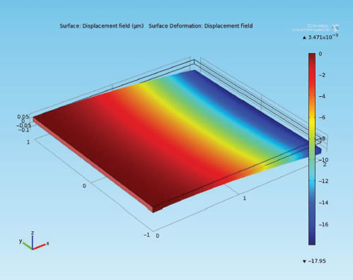
One example of COMSOL results is shown in the figure. This figure was from a model that included a gradient in the piezoelectric constant that couples the zaxis electric field to the x-axis strain. This particular model included the x = 0 surface constrained in the x direction. In addition to the negative curvature in the xz plane, there is a slight positive curvature in the yz plane. This curvature is seen from the curved lines of equal z-axis displacement, and results from Poisson’s ratio. Poisson’s ratio for a material relates the strain in one direction to the negative strain in the orthogonal direction. To confirm this explanation, another model was run with Poisson’s ratio set to zero. The resulting surface had the lines of constant z-displacement straight and parallel to the y-axis.
Of the 18 evaluation samples provided, one sample has been briefly assessed by allowing the sample to hang freely and applying voltages to the electrodes. In contrast with previous films, this film showed very little deformation, even with the application of 4.5 kV. A laser was used to measure the angle of the surface deflection, with the deflection equal to roughly 5º at 3 kV. This is the order of magnitude of response expected when the film is constrained at the edges. There are several potential explanations for the behavior. The difference could be due to the smaller sample size and the linear configuration (previous films were substantially larger and circular), reducing the effects of the border around the active area of the film.
This work was done by Greg A. Finney of Kratos Defense and Security Solutions for the Office of Naval Research. ONR-0025
More From SAE Media Group
Tech Briefs
X-Ray Crack Detectability
Electronics & Sensors INSIDER
Researchers Have Developed the World’s Smallest Ultrasound Detector
Electronics & Sensors INSIDER
Manufacturing the World's Tiniest Light-Emitting Diodes
Photonics & Imaging Technology
Silicon Carbide Optics for High-Energy Applications
Photonics & Imaging Technology
Advancements Make Laser-Based Imaging Simpler and Three-Dimensional
Photonics & Imaging Technology
Seeing Like a Butterfly: Optical Invention Enhances Camera Capabilities
Photonics & Imaging Technology
The Hidden Effects of Optical Coating Stress
Tech Briefs
Multi-Spectral Imaging Pyrometer
Photonics & Imaging Technology
Measuring Surface Roughness with an Atomic Force Microscope
Photonics & Imaging Technology
Sharper Images: A Breakthrough in Microscopy Resolution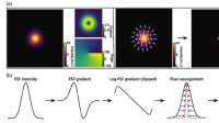
Photonics & Imaging Technology INSIDER
AI Image Analysis, Li-Fi and Quantum Processor Among 2023 PRISM Awards Winners
Automotive Engineering
A Cool New Dimension to Automotive Plastics’ Testing
Photonics & Imaging Technology
Additive Manufacturing of Precision Optics at Micro and Nanoscale
Medical Design Briefs
Ultra-Sensitive, Small Optomechanical Ultrasound Sensor
Motion Design
Liquid Crystals Hold the Key to Shapeshifting Robots
Tech Briefs
Technique Enables 3D Printing of Microstructures


Photonics & Imaging Technology
2021 OEM Photonics & Imaging Directory
Photonics & Imaging Technology INSIDER
New Product Launches and Technologies to See at Photonics West 2025
Photonics & Imaging Technology
Deformation Fingerprints Will Help Researchers Identify, Design Better Metallic Materials
Tech Briefs
Sub-Pixel Spatial Resolution Interferometry
Photonics & Imaging Technology
SPIE Photonics West 2019 Preview
Photonics & Imaging Technology
Machine Vision Applications in Laser Measurement Systems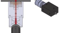
Photonics & Imaging Technology
Individual Quantum Dots Imaged in 3-D for the First Time
Photonics & Imaging Technology
Spider Silk Can Create Lenses Useful for Biological Imaging
Photonics & Imaging Technology
ZERODUR: The Highly Technical Glass-Ceramic
Top Stories
INSIDERDefense
![]() New Raytheon and Lockheed Martin Agreements Expand Missile Defense Production
New Raytheon and Lockheed Martin Agreements Expand Missile Defense Production
NewsAutomotive
![]() Ford Announces 48-Volt Architecture for Future Electric Truck
Ford Announces 48-Volt Architecture for Future Electric Truck
INSIDERManufacturing & Prototyping
![]() Active Strake System Cuts Cruise Drag, Boosts Flight Efficiency
Active Strake System Cuts Cruise Drag, Boosts Flight Efficiency
ArticlesTransportation
![]() Accelerating Down the Road to Autonomy
Accelerating Down the Road to Autonomy
INSIDERMaterials
![]() How Airbus is Using w-DED to 3D Print Larger Titanium Airplane Parts
How Airbus is Using w-DED to 3D Print Larger Titanium Airplane Parts
Road ReadyTransportation
Webcasts
Electronics & Computers
![]() Cooling a New Generation of Aerospace and Defense Embedded...
Cooling a New Generation of Aerospace and Defense Embedded...
Power
![]() Battery Abuse Testing: Pushing to Failure
Battery Abuse Testing: Pushing to Failure
Connectivity
![]() A FREE Two-Day Event Dedicated to Connected Mobility
A FREE Two-Day Event Dedicated to Connected Mobility
Automotive
![]() Quiet, Please: NVH Improvement Opportunities in the Early Design Cycle
Quiet, Please: NVH Improvement Opportunities in the Early Design Cycle
Transportation
![]() Advantages of Smart Power Distribution Unit Design for Automotive &...
Advantages of Smart Power Distribution Unit Design for Automotive &...
Aerospace
![]() Sesame Solar's Nanogrid Tech Promises Major Gains in Drone Endurance
Sesame Solar's Nanogrid Tech Promises Major Gains in Drone Endurance