


Threshold Voltage Tuning of Metal-Gate MOSFETs Using an Excimer Laser
This technique enables tailored threshold voltage on a device-to-device basis for greater design flexibility.
This work presents a localized method for tuning the threshold voltages (Vt) of multilayer metal-gate metal-oxide-semiconductor field-effect transistor (MOSFET) devices with a spatial area theoretically limited by the wavelength of the laser beam. This technique allows an independent means to tailor threshold voltage on a device-to-device basis that provides greater design flexibility. This maskless technique allows tailoring of thresholds by tuning the work function of the gate by intermixing titanium and titanium nitride using a laser pulse. The source and drains of the MOSFET are simultaneously annealed by the laser.
The process for tuning the threshold voltage occurs after the metal-gate stack is formed via physical vapor deposition (PVD), and the source and drain of the MOSFET have undergone ion implantation. At this point, the device is irradiated with a series of laser pulses to anneal the source and drain regions, while the majority of the laser energy impinging on the gate region is reflected off the metal gate. The substrate is preferably silicon-on-insulator (SOI) to facilitate higher temperatures near the gate interface in comparison to bulk Si.
A self-aligned process is used to fabricate metal-gate MOSFET devices on a single SOI wafer formed by Separation-by-Ion-Implantation-of-OXide (SIMOX). The multilayer metal gate of the self-aligned MOSFET was formed by PVD of 10-nm titanium (Ti), followed by 50 nm of titanium nitride (TiN) and 200-nm Al on top of a 7.5-nm gate oxide formed by dry oxidation.
After source and drain implantation, the devices were irradiated with a 308-nm XeCl excimer laser at a fluence (energy density) of 415 mJ/cm2. Each laser pulse normally occurs on a time scale of 10 to 30 ns and activates the source and drain dopants, as well as initiating thermal mixing. The TiN layer intermixes with the bottom Ti layer as a result of N diffusion at 800 °C temperatures. This intermixing causes the work function of Ti (4.33 eV) to shift towards the work function of TiN (4.55 eV), directly increasing the threshold voltage. The laser-induced thermal activation of channel dopants also contributes to the Vt increase as a smaller second-order effect for a larger number of laser pulses.
The threshold voltage was obtained using the traditional linear extrapolation method at the point of maximum slope. A typical error of ±0.01 eV is assigned to each data point to account for discrepancies in the fabrication process. The threshold voltage exhibits a linear shift of 70 mV from 0.32 to 0.39 V over 20 laser pulses, which is controlled by the laser fluence and the number of pulses. A poly-Si gate transistor was fabricated for comparison. In this situation, the majority of the laser irradiation of the poly-Si gate is absorbed in the gate.
This work was done by R.P. Lu, A.D. Ramirez, B.W. Offord, and S.D. Russell of SPAWAR Systems Center Pacific for the Office of Naval Research. For more information, download the Technical Support Package (free white paper) at www.defensetechbriefs.com/tsp under the Photonics category. ONR-0017
More From SAE Media Group
Photonics Tech Briefs
Fabrication of Robust, Flat, Thinned, UVImaging CCDs
Aerospace & Defense Tech Briefs
Laser Integration on Silicon Photonic Circuits Through Transfer Printing
Aerospace & Defense Tech Briefs
On the Pulsed Laser Ablation of Metals and Semiconductors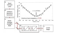
Imaging Technology
Design and Fabrication of High-Efficiency CMOS/CCD Imagers
Photonics Tech Briefs
Precise Stabilization of the Optical Frequency of WGMRs
Aerospace & Defense Tech Briefs
Fabrication and Electrical Characterization of Correlated Oxide Field Effect Switching Devices for High Speed Electronics
Photonics Tech Briefs
Etching Mirror Facets on SOI Optical Waveguides
Photonics & Imaging Technology
Fiber Lasers for Powertrain Welding Applications
Photonics & Imaging Technology
Industrial Blue Lasers
Air Force Research Laboratory Technology Horizons
Patterned Gallium Arsenide Devices for Infrared Countermeasures
Tech Briefs
New Family of Glass for Lens Applications
Photonics Tech Briefs
Delta-Doped Hybrid Advanced Detector


Photonics Tech Briefs
Lateral-Current-Collection HgCdTe Infrared Detectors
Photonics & Imaging Technology
Upside-Down Design Expands Wide-Spectrum Super-Camera Abilities
Photonics Tech Briefs
Optical Processing Furnace
Photonics & Imaging Technology
Nanoscale Machines Convert Light into Work
Photonics & Imaging Technology
A Sharper Look at the Interior of Semiconductors
Photonics & Imaging Technology
R&D Effort Produces Magnetic Devices to Enable More Powerful X-ray Lasers
Photonics Tech Briefs
Back-Illuminated CCDs With Integral Ultraviolet-Pass Filters

Aerospace & Defense Tech Briefs
Integrated Magneto-Optical Devices for On-Chip Photonic Systems
Photonics & Imaging Technology
Blue Lasers: Leveraging Fundamental Physics for High Performance
Photonics Tech Briefs
Photodiode-Based CMOS APSs With Zero-Lag, Low-Noise, High-Linearity Design
Photonics & Imaging Technology
Optimizing Laser Cutting in Semiconductor Advanced Packaging

Tech Briefs
High-Efficiency Laser for Silicon Chips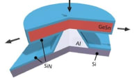
Tech Briefs
Hybrid Material is an Efficient Photodetector
Top Stories
INSIDERManufacturing & Prototyping
![]() How Airbus is Using w-DED to 3D Print Larger Titanium Airplane Parts
How Airbus is Using w-DED to 3D Print Larger Titanium Airplane Parts
INSIDERManned Systems
![]() FAA to Replace Aging Network of Ground-Based Radars
FAA to Replace Aging Network of Ground-Based Radars
NewsTransportation
![]() CES 2026: Bosch is Ready to Bring AI to Your (Likely ICE-powered) Vehicle
CES 2026: Bosch is Ready to Bring AI to Your (Likely ICE-powered) Vehicle
NewsSoftware
![]() Accelerating Down the Road to Autonomy
Accelerating Down the Road to Autonomy
EditorialDesign
![]() DarkSky One Wants to Make the World a Darker Place
DarkSky One Wants to Make the World a Darker Place
INSIDERMaterials
![]() Can This Self-Healing Composite Make Airplane and Spacecraft Components Last...
Can This Self-Healing Composite Make Airplane and Spacecraft Components Last...
Webcasts
Defense
![]() How Sift's Unified Observability Platform Accelerates Drone Innovation
How Sift's Unified Observability Platform Accelerates Drone Innovation
Automotive
![]() E/E Architecture Redefined: Building Smarter, Safer, and Scalable...
E/E Architecture Redefined: Building Smarter, Safer, and Scalable...
Power
![]() Hydrogen Engines Are Heating Up for Heavy Duty
Hydrogen Engines Are Heating Up for Heavy Duty
Electronics & Computers
![]() Advantages of Smart Power Distribution Unit Design for Automotive...
Advantages of Smart Power Distribution Unit Design for Automotive...
Unmanned Systems
![]() Quiet, Please: NVH Improvement Opportunities in the Early Design...
Quiet, Please: NVH Improvement Opportunities in the Early Design...