


Integrated Magneto-Optical Devices for On-Chip Photonic Systems
Development of magneto-optical (MO) materials could lead to a range of nonreciprocal optical devices for emerging standardized photonic integrated circuit (PIC) fabrication processes.
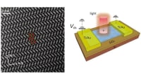
The magneto-optical (MO) oxide layer consists of (Bi,Y)3Fe5O12 or BiYIG, bismuth garnet. This material was selected because it has a better figure of merit than the CeYIG previously used, especially at lower wavelengths (1310 nm vs. 1550 nm). A top-down deposition process was developed in which BiYIG/YIG stacks are grown on the Si waveguide with YIG on top. The stack is annealed at 800°C/5 min to crystallize both layers, with the YIG templating the BiYIG leading to garnet phases rather than other oxides, and the BiYIG is directly on the Si waveguide. Initial attempts led to a film with Bi oxide phases, because the Bi was in excess and could not escape during the anneal as occurs in Si/YIG/BiYIG stacks. Hence the composition was adjusted to include slightly more Fe, which yielded films with only garnet peaks.
Conditions were also developed for growth of Bi-substituted iron garnet (BiYIG) on GGG garnet and Si substrates by combinatorial pulsed laser deposition.

For single crystal films on GGG (Figure 1), the conditions for growth that produced films with the best saturation magnetization (Ms) and surface topography were found to be at higher temperatures of 520-560°C and at oxygen pressures of 10 to 20 mTorr. Structural characterization revealed the growth of epitaxial BiYIG film on GGG without any secondary phases. This result was further confirmed by compositional analysis that showed the ratio of Bi+Y/Fe, as expected, was approximately 0.6 (in the range 0.62-0.65) suggesting no formation of secondary ferrous phases. The FR was 1.5 °/μm, which is comparable to other work considering the Bi content. The saturation field for out of plane hysteresis or Faraday loops is ~2 kOe which is close to that expected just from shape anisotropy, i.e. magne-tocrystalline or magnetoelastic contributions to anisotropy are probably small.
For polycrystalline films on Si (Figure 2) top-down crystallization of BiYIG using a YIG seed layer on topographical substrates was carried out to promote the crystallization of BiYIG on photonic substrates. A bilayer was grown (YIG/BiYIG/substrate) at 650°C, then annealed at 800°C. With the top seed layer, Bi escape during annealing was suppressed and the composition had to be adjusted (less Fe was added) to avoid secondary phases.

X-ray diffraction (XRD) showed crystallization to the garnet structure and the saturation magnetization was consistent with the film thickness and the bulk magnetization of YIG and BiYIG (which are similar). However, films on Si had much weaker FR than expected.
During this work, the pulsed-laser deposition (PLD) system was reconfigured leading to a higher intensity of light incident on the target and higher growth rates, which led to a change in composition of most materials deposited by PLD. Compositional analysis showed that more recent BiYIG films contained less Bi than before, and this may account for the lower FR. The target, which contained Bi:Y:Fe = 0.8:2.2:5, yielded films of 0.5:2.5:3.8, or 0.5:1.9:4.2 when additional Fe oxide was code-posited. (In the latter case, Bi+Y/Fe = 0.57 which matches the stoichiometric ratio of 3/5 = 0.6.)
The results of growth experiments indicate that films grow with garnet crystal structure on GGG, even if the Bi+Y/Fe stoichiometry is not exactly correct. However, growth on Si is less forgiving, and making good quality garnet requires a closer control of stoichiometry. The Bi:Y ratio is controlled mainly by temperature, and the Bi+Y/Fe ratio is sensitive to laser power.
This work was done by Caroline Ross and Juejun Hu, Massachusetts Institute of Technology for the Air Force Research Laboratory. AFRL-0264
This Brief includes a Technical Support Package (TSP).
Integrated Magneto-Optical Devices for On-Chip Photonic Systems
(reference AFRL-0264) is currently available for download from the TSP library.
Don't have an account?
More From SAE Media Group
Aerospace & Defense Tech Briefs
Fabrication and Electrical Characterization of Correlated Oxide Field Effect Switching Devices for High Speed Electronics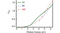

Photonics & Imaging Technology
Silicon Carbide Optics for High-Energy Applications

Photonics & Imaging Technology
Measuring Surface Roughness with an Atomic Force Microscope
Tech Briefs
5 Ws of Invisible Glass
Aerospace & Defense Tech Briefs
Reconfigurable Electronics Based on Multiferroics and Nanomagnetism
Electronics & Sensors INSIDER
Manufacturing the World's Tiniest Light-Emitting Diodes

Photonics & Imaging Technology
Additive Manufacturing of Precision Optics at Micro and Nanoscale
Aerospace & Defense Tech Briefs
3D Meta-Optics for High-Energy Lasers
Photonics & Imaging Technology
Military Optics Technology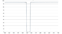

Tech Briefs
“Light-Written” Photonic Memory Devices
Aerospace & Defense Tech Briefs
Streamlined Microcomb Design Provides Control With The Flip of a Switch
Photonics & Imaging Technology
Researchers Create World’s Smallest LED And Holographic Microscope
Photonics & Imaging Technology
Moving Precision Communication, Metrology, Quantum Applications from Lab to Chip
Aerospace & Defense Tech Briefs
Low Power Optical Phase Array Using Graphene on Silicon Photonics
Tech Briefs
3D Inks Can Be Erased Selectively
Tech Briefs
Chip Measures Quantities with Quantum Precision

Aerospace & Defense Tech Briefs
Epitaxial Growth of Rhenium with Sputtering
Photonics & Imaging Technology
Photonic Integrated Circuit Testing: Accelerating R&D From Lab to Fab
Aerospace & Defense Tech Briefs
Ultracompact, High-Speed Field-Effect Optical Modulators
Tech Briefs
Material Increases Efficiency of LED Devices
Photonics & Imaging Technology
Researchers Create Precision Optical Components with Inkjet Printing
Photonics & Imaging Technology
Optical Coatings Technology

Photonics & Imaging Technology
A First-Of-Its-Kind Integrated Optical Isolator
Overview
The document titled "Integrated Magneto-Optical Devices for On-Chip Photonic Systems" is a final report detailing research conducted under the sponsorship of the Air Force Research Laboratory (AFRL) and the Defense Advanced Research Projects Agency (DARPA). The research, carried out from May 3, 2016, to May 3, 2017, focuses on the development of magneto-optical (MO) materials aimed at enabling nonreciprocal optical devices for photonic integrated circuits (PICs).
The primary objective of the program was to create MO materials that can be integrated into various optical and radio frequency (RF) photonic devices. These devices include low-loss interconnect waveguides, power splitters, filters, active amplifiers, lasers, optical modulators, and photodetectors. The report outlines the design of resonator and Mach-Zehnder interferometer (MZI) isolator devices, which were developed through optical modeling for both transverse-electric (TE) and transverse-magnetic (TM) polarization.
The document is structured into several sections, beginning with a summary of key project results, followed by a detailed research description. It discusses the development of magneto-optical materials, the design of isolators, waveguide fabrication, and device characterization. The findings highlight the potential of these integrated magneto-optical devices to enhance the performance and functionality of on-chip photonic systems.
The report emphasizes the significance of these advancements in the context of standardized PIC fabrication processes, which are crucial for the future of optical communication and signal processing technologies. The research contributes to the understanding of how magneto-optical materials can be utilized to create efficient and effective optical devices that can operate in various applications.
Overall, the report serves as a comprehensive resource for researchers and professionals in the field of photonics, providing insights into the development and application of magneto-optical devices. It underscores the importance of continued research in this area to drive innovation in photonic systems, which are increasingly vital in modern communication and information technologies. The document is unclassified and approved for public release, making it accessible for further study and exploration by interested parties.
Top Stories
INSIDERAerospace
![]() How Airbus is Using w-DED to 3D Print Larger Titanium Airplane Parts
How Airbus is Using w-DED to 3D Print Larger Titanium Airplane Parts
NewsUnmanned Systems
![]() Microvision Aquires Luminar, Plans Relationship Restoration, Multi-industry Push
Microvision Aquires Luminar, Plans Relationship Restoration, Multi-industry Push
INSIDERRF & Microwave Electronics
![]() A Next Generation Helmet System for Navy Pilots
A Next Generation Helmet System for Navy Pilots
ArticlesUnmanned Systems
![]() Accelerating Down the Road to Autonomy
Accelerating Down the Road to Autonomy
INSIDERDesign
![]() New Raytheon and Lockheed Martin Agreements Expand Missile Defense Production
New Raytheon and Lockheed Martin Agreements Expand Missile Defense Production
ArticlesUnmanned Systems
![]() CES 2026: Bosch is Ready to Bring AI to Your (Likely ICE-powered) Vehicle
CES 2026: Bosch is Ready to Bring AI to Your (Likely ICE-powered) Vehicle
Webcasts
Automotive
![]() Advantages of Smart Power Distribution Unit Design for Automotive...
Advantages of Smart Power Distribution Unit Design for Automotive...
Transportation
![]() Quiet, Please: NVH Improvement Opportunities in the Early Design...
Quiet, Please: NVH Improvement Opportunities in the Early Design...
Electronics & Computers
![]() Cooling a New Generation of Aerospace and Defense Embedded...
Cooling a New Generation of Aerospace and Defense Embedded...
Automotive
![]() Battery Abuse Testing: Pushing to Failure
Battery Abuse Testing: Pushing to Failure
Connectivity
![]() A FREE Two-Day Event Dedicated to Connected Mobility
A FREE Two-Day Event Dedicated to Connected Mobility