Image Sensors and Cameras Based on Colloidal Quantum Dots for Defense Applications
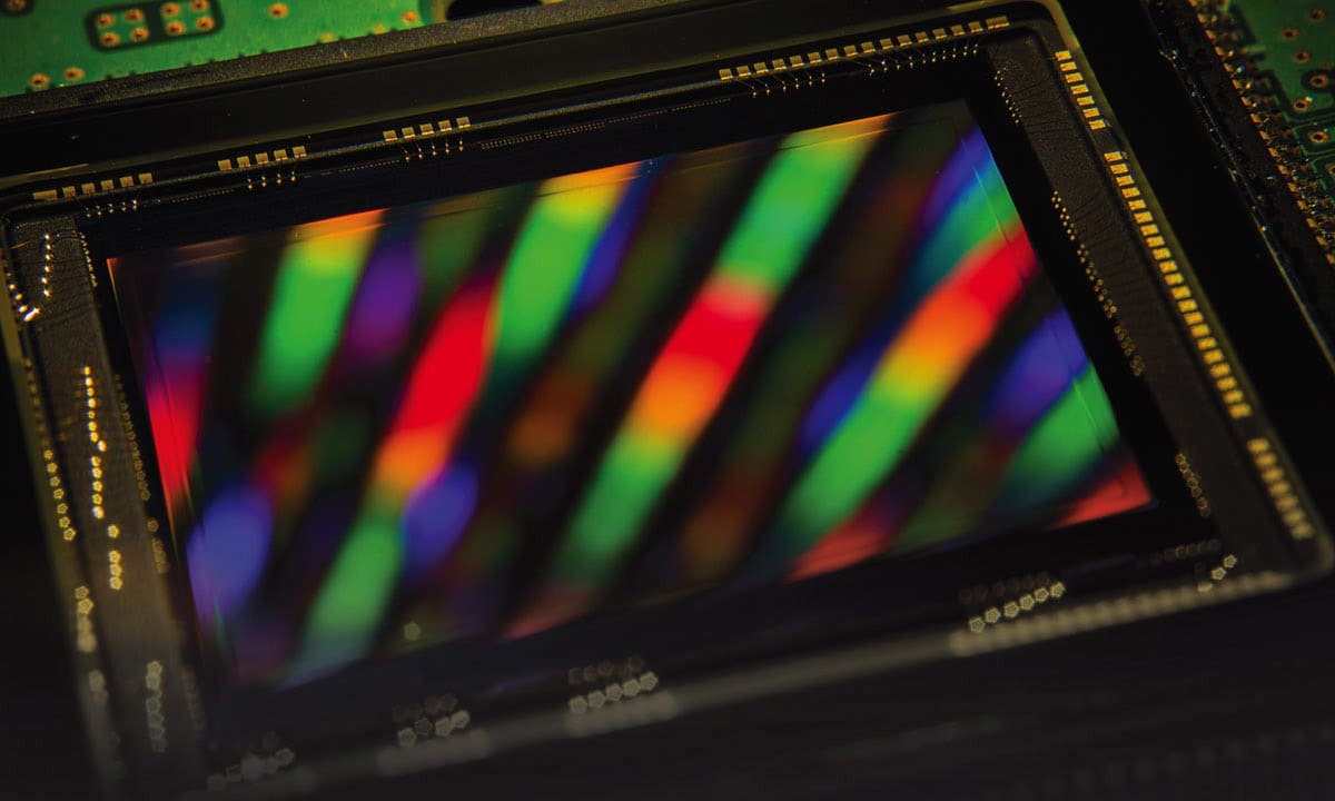
Colloidal quantum dot (CQD) -based image sensors accomplish several advantageous and unique features such as tailorable wavelength response via selection of dot size and material system, monolithic integration by processing directly onto the CMOS wafer surface thus avoiding hybridization cost and complexity, and scalability in pixel dimensions and density, whereby the limitations are primarily set by the resolution of the underlying CMOS process. Major efforts and successes have been reported in recent years by several academic groups and industrial entities in the research and development of CQD image sensors and their monolithic integration on CMOS platforms. To achieve uniform and defect-free imagers performing at high speed with low read-out noise, the entire system from ROIC front-end to wafer surface planarization to pixel stack structure, must be optimized as a whole; this is the approach Emberion has pursued with our in-house ROIC design and end-to-end fabrication process development.
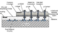
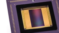
This article reports on the image sensor technology and the VS20 camera product developed at Emberion. The article does this by describing the image sensor design comprising the sensor stack based on a p-i-n photodiode implementation with PbS QDs sandwiched between thin-film hole transport (HTL) and electron transport (ETL) layers as well as the CMOS ROIC architecture and pixel front-end interfacing the photodiode stack. Further on, the functionalities of the camera are described at hardware (HW) and software (SW) level including a brief introduction of the image processing pipeline (IPP) implementation. Next, we outline the image sensor fabrication process involving wafer planarization steps and photosensor stack processing including CQD deposition and ligand exchange steps.
Image Sensor and Camera Design
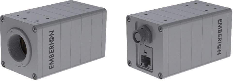
The VS20 camera has been entirely custom-designed in-house at Emberion including the image sensor IC, sensor material stack design, sensor package, camera circuitry and mechanics, as well as the camera FW/SW including the image processing pipeline (IPP) and user-interface (UI). This way, it has been possible to optimize the interface between the CQD-based pixel stack and read-out circuitry and maintain full design versatility from imager to camera design.
Quantum dots provide a means to engineer device structures exhibiting unique optical and electronic properties beneficial to numerous practical applications. With material dimensions reduced to around 1 to 20 nm in diameter, the effective bandgap of the semiconductor becomes size dependent resulting from quantum confinement. Here, we utilize PbS quantum dots as the optical absorbing material. At a nominal diameter of 8 nm, the excitonic absorption peak resides at ca. 1,800 nm and the resulting device stack exhibits photoresponsivity from visible to SWIR with a cut-off wavelength at ca. 2,000 nm. Similarly to many literature reports, we employ bulky surface ligands to sterically stabilize the QDs as a colloidal dispersion during wet-deposition by spin-coating. A sequence of chemical treatments is subsequently carried out to interchange the long-chain insulating molecules for shorter and conductive ligands facilitating the QDs to self-organize into a densely packed matrix with favorable coupling and charge transport characteristics.

Image Sensor ROIC
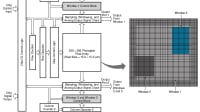
The Emberion designed ROIC architecture supports modularity and enables functionalities for different types and sizes of arrays and pixels according to application requirements. The ROIC contains a system-on-chip (SoC) solution corresponding to the block diagram presented in Figure 2(a). Here, the sequencer controls the exposure and reset times, trigger synchronization, and other features such as HW-level regions of interest (ROI). The ROIC is controlled via the serial peripheral interface (SPI) from a camera core. A base sequence is pre-programmed into the ROIC’s ROM enabling image / video acquisition immediately upon power-up. The sequencer is re-programmable via SPI to support more advanced sequences when needed. Differential analog high-speed buffers output the signal to an external analog-to- digital converter (ADC) located on the camera front-end board. The image sensor ROIC reported here supports VGA resolution with 20 um pixel pitch and 15.0 × 12.4 mm2 overall imager die size with IO-ring included.

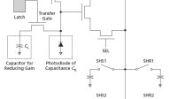
The p-i-n type photodiode structures can be read-out either in current-mode (Figure 2(b)), where the photodiode is typically reverse-biased, or in voltage-mode (Figure 2(c)), where the forward-voltage across the photodiode increases as a function of photogenerated charge eventually reaching open-circuit voltage in the case of sufficiently long exposure time. The input impedance of the pixel electronics is in the TΩ range so that minimal charge leakage occurs during exposure, whilst, between exposure cycles, the photodiode is reset by short-circuiting the photodiode stack thus discharging any photogenerated charge between successive frames. The VGA imager reported here has been optimized to operate in voltage-mode over a wide range of exposure times achieving above 400 fps for full VGA resolution with minimum exposure time of 1 μs. The input-referred read-out noise level at the pixel front-end is ~180 μV. The signal path gain from pixel electrode to ASIC differential output is adjustable (0 to 29.5 dB) and currently optimized to yield G ≈ 8 for pixel voltages 0 to 100 mV.
Looking beyond the work reported here, our latest generation ROIC supports up to 1.3 MPixel array size with minimum pixel pitch of 10 μm, where the dual-mode pixel front-end accommodates for either voltage or current-mode measurement, the latter with reverse-biased stack and CTIA design.
Camera Design and IPP
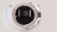
The VS20 Core/Compact product was first demonstrated at Photonics West 2024 to complement Emberion’s camera offering with a form-factor optimized for system integration. The camera solution incorporates all necessary functionalities for sensor readout, control, analog-to-digital signal conversion, image pre-processing, thermal control, power management and GigE Vision interface capable of frame rates up to and above 400 fps. Stable performance over a wide operational temperature range is ensured with a thermo-electric cooling (TEC) element built in the image sensor package. For the stand-alone camera, the circuit boards are supplemented by housing designed for efficient thermal management and protection against dust intrusion. The VS20 Core/Compact is compatible with commercial lens systems with a standard C-mount optical interface. The back cover has power/trigger and RJ45 ethernet connectors.
The camera functional block diagram is shown in Figure 2(d) and a 3D CAD model of the VS20 Core is shown in Figure 2(e). The image sensor and internal TEC and thermistor are housed inside a 28-pin hermetically sealed metallic sensor package with a double-side anti-reflection (AR) coated Sapphire glass window providing >90 percent transmission over the wavelength range 400 to 2,500 nm. A custom-designed ceramic interposer provides routings from the IO ring pads on the sensor to the output pins on the package. The ADCs on the sensor front-end board digitize the VGA sensor’s differential output signal as well as the voltage over thermistor for TEC control. The TEC controller is bi-directional so that the sensor can be cooled and heated. The main component of the processing board is the SoC processor comprised of a dual-core Cortex-A53 and a dual-core Cortex-R5 real-time processing unit mated with programmable logic. DDR memory is used as a frame buffer for the image frames read from the sensor. Real-time image processing takes place in the ARM processor/FPGA depending on the set frame rate. Under typical use-case conditions, the camera power consumption remains below 12 W for operation up to 400 fps.
Fabrication, Assembly and Measurement
The Emberion in-house designed imager circuit is taped-out and manufactured at a semiconductor foundry. The CMOS wafers are then planarized using a sequence of post-process steps to achieve a surface profile optimal for the latter CQD stack process steps. The absorber stack is processed in-house using Emberion’s custom-built pilot manufacturing line including wet-deposition, sputtering, evaporation, and ALD process steps. The image sensors are measured at wafer-level before die selection and packaging assembly. Finally, the packaged imager is assembled into the camera for camera testing and measurement.
Wafer Post-Process

The image sensor ROICs are fabricated on 200 mm wafers using a standard 180 nm node CMOS foundry process. The as-received CMOS wafers require planarization so that deposition of uniform and high-quality thin-film photodiode layers is possible. The Damascene planarization process is used here to achieve maximum step heights below 50 nm across the pixel array and exhibiting at most 200 nm dishing at the IO pad ring and saw lane regions. Pixel electrodes with below 50 nm thickness are sputter-deposited and lithographically patterned onto the planarized wafer surface. Figure 3(a) shows the visual appearance of the wafer after planarization and metallization steps. The typical features of the pixel electrodes and vias prior to stack processing are displayed in Figure 3(b-c).
Device Assembly and Characterization
Following the image sensor stack fabrication, the processed wafers are measured on a semi-automated probe station using a custom-built probe card setup incorporating all relevant camera electronics and features including a lens mount fixture. This way, comprehensive functionality and performance evaluation of each image sensor die is completed prior to dicing and packaging steps. Relevant figures of merit (FoM) are extracted from the measurement data including photosensitivity and deviation metrics with associated threshold levels for die selection. The die pick map is created based on the array measurement results complemented with inspection data and microscope images from the fabrication process. Furthermore, additional PCM test structures including isolated test pixels are measured using a semiconductor parameter analyzer enabling current-voltage (J-V) and capacitance-voltage (C-V) measurement from the p-i-n photodiode stack. The image sensor dies are singulated by wafer sawing with front-side protective film.

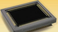
Each selected image sensor die is packaged into a metallic package with pre-assembled TEC and interposer components. The packaging assembly involves die attach, wire bonding, vacuum dehydration and sealing steps. The hermetically sealed packages are leak tested according to MIL-spec. Figure 4(a-b) shows the metallic package before and after die assembly and lid closure. The packaged imagers are further assembled into the VS20 camera core mechanics ensuring good thermal contact to the sensor package base for efficient heat sinking (Figure 4(c-d)).
The camera testing is carried out in the following stages: (i) performance testing under uniform illumination including wavelength sweep, irradiance sweep, and exposure-time sweep characterization, (ii) calibration under uniform light with broadband illumination, and (iii) imaging tests with lens objectives and test charts with calibration, including non-uniformity correction (NUC), applied. Figure 4(e) shows one of the tunable wavelength test setups employed at Emberion enabling testing over the wavelength range 400 nm to 2,500 nm with adjustable attenuation via the neutral density (ND) filters. Here, the VS20 is positioned so that the image sensor is at the exit port of the integrating sphere. A reference detector is positioned at an adjacent exit port and functions as a calibration reference. The same setup is used for the calibration whilst separate setups are employed for measuring the dynamic response of the sensor and for the test chart imaging.
Applications
SWIR imaging is relevant for numerous applications across various industries including defense and surveillance, machine vision, industrial automation, quality control, medical imaging, automation, and for example augmented reality within the consumer domain. Taking advantage of the broad spectrum, Emberion cameras can detect all the laser range finder wavelengths (905 nm, 1,064 nm, 1,550 nm, >1,700 nm) providing tactical advantage. With HDR > 120 dB, surveillance is a prime application including seeing through adverse conditions such as smoke, haze, and snow.
One of the keys areas of application is in Defense where Emberion’s QD sensor based cameras can be used for surveillance i.e. in harsh environments (snow, haze, smoke). In addition to this, a camera that can detect all the laser wavelengths for laser range finding and designation is vital i.e. 905 nm, 1,064 nm, 1,550 nm and beyond 1,700 nm for tactical advantage. It can support camouflage detection and using wavelength >1,850 nm and taking advantage of the 1,920-1,940 nm water peak it can detect the appropriate contrast level required to detect objects.
Conclusion
Imagers based on CQD-on-CMOS are emerging as a competitively performing and cost-effective alternative to Indium Gallium Arsenide (InGaAs) currently dominant in SWIR sensing. The tailorable spectral range and scalability in pixel dimensions provide opportunities for next-level application-specific optimization. When comparing focal plane arrays (FPAs), the relevant FoM providing best like-for-like performance comparison is NEI, which indicates the actual sensitivity performance of the array at a given target frame rate. Although InGaAs sensors exhibit external quantum efficiency (EQE) superior to CQD, and low dark current in the range of few fA, the NEI performance is limited by read- out noise typically of the order of 250 e- for CTIA-based ROICs. Our preliminary calculations indicate that the NEI- performance of Emberion’s VGA imager with 20 μm pixel size exceeds that of benchmark 5 μm-pixel InGaAs imagers.
This article was written by Mark Allen, Chief Technology Officer, Emberion (Espoo, Finland), in collaboration with a team of engineers and researchers from Emberion. Some of the material was featured in a paper presented by the Emberion team at the 2024 SPIE Defense + Commercial Sensing Conference. For more information, visit here .
Top Stories
NewsRF & Microwave Electronics
![]() Microvision Aquires Luminar, Plans Relationship Restoration, Multi-industry Push
Microvision Aquires Luminar, Plans Relationship Restoration, Multi-industry Push
INSIDERAerospace
![]() A Next Generation Helmet System for Navy Pilots
A Next Generation Helmet System for Navy Pilots
INSIDERDesign
![]() New Raytheon and Lockheed Martin Agreements Expand Missile Defense Production
New Raytheon and Lockheed Martin Agreements Expand Missile Defense Production
INSIDERMaterials
![]() How Airbus is Using w-DED to 3D Print Larger Titanium Airplane Parts
How Airbus is Using w-DED to 3D Print Larger Titanium Airplane Parts
NewsPower
![]() Ford Announces 48-Volt Architecture for Future Electric Truck
Ford Announces 48-Volt Architecture for Future Electric Truck
ArticlesAR/AI
Webcasts
Electronics & Computers
![]() Cooling a New Generation of Aerospace and Defense Embedded...
Cooling a New Generation of Aerospace and Defense Embedded...
Automotive
![]() Battery Abuse Testing: Pushing to Failure
Battery Abuse Testing: Pushing to Failure
Power
![]() A FREE Two-Day Event Dedicated to Connected Mobility
A FREE Two-Day Event Dedicated to Connected Mobility
Unmanned Systems
![]() Quiet, Please: NVH Improvement Opportunities in the Early Design Cycle
Quiet, Please: NVH Improvement Opportunities in the Early Design Cycle
Automotive
![]() Advantages of Smart Power Distribution Unit Design for Automotive &...
Advantages of Smart Power Distribution Unit Design for Automotive &...
Energy
![]() Sesame Solar's Nanogrid Tech Promises Major Gains in Drone Endurance
Sesame Solar's Nanogrid Tech Promises Major Gains in Drone Endurance

