


FPGA-Based Communication Channel for Digital Signal Processor Chips
Use of FPGAs eliminates cables when connecting DSPs.
A method for networking, and a network of, digital signal processors (DSP) via at least one field-programmable gate array (FPGA) enables the simultaneous broadcast of data from a DSP to a number of DSPs. The apparatus comprises a host DSP, at least one FPGA in communication with the host DSP for receiving a digital signal from the host DSP, and at least one non-host DSP in communication with at least one FPGA for receiving the digital signal.
The number of non-host DSPs receiving data broadcast from the host DSP may be greater than the number of communication ports located on the host DSP. The networking method does not require each non-host DSP to be physically connected to the host DSP. This is achieved by interposing an FPGA between the host DSP and the non-host DSPs. The FPGA serves to receive the broadcast data from the host DSP, to buffer the data received, and to handle the communication and dissemination of the buffered broadcast data to multiple non-host DSPs.
The host DSP is housed within a host computer, preferably a PC. The host DSP is in communication with the FPGA via a connection that connects a communication port located on the host DSP to a communication port located on the FPGA. Connection provides bidirectional communication between the host DSP and the FPGA. The FPGA has multiple additional communication ports, which are utilized to communicate with a multitude of additional non-host DSPs. The FPGA communicates with each non-host DSP via a connection that connects a single communication port located on the FPGA to a single communication port located on a non-host DSP. In this manner, bidirectional communication is enabled between each non-host DSP and the FPGA.
In operation, the host DSP communicates a single stream of data to the FPGA via a connection. It is a property of FPGAs that they may be dynamically programmed to execute software instructions. The FPGA is therefore programmed to buffer the stream of data received by the host DSP and to transmit the received and buffered data out via the plurality of communication ports in communication with non-host DSPs. In addition to transmitting the buffered data, the FPGA is preferably programmed to perform any and all initialization and data synchronization activities required to facilitate the communication of buffered data between the FPGA and all non-host DSPs. Such communication may be either synchronous or asynchronous.
The FPGA is constructed to comprise an internal memory capable of storing, retrieving, and returning upon request, digital data. The FPGA may be in communication with an external storage device wherein the data broadcast by the host DSP to the FPGA may be buffered and stored in external storage device, and retrieved by the FPGA as required for broadcast to the non-host DSPs.
In addition to communicating with non-host DSPs, the FPGA may similarly communicate with a peripheral device via a communication port located on the FPGA and connected to the peripheral device.
This work was done by C. Ray Dutton of the Naval Undersea Warfare Center.
NUWC-0003
This Brief includes a Technical Support Package (TSP).
FPGA-Based Communication Channel for Digital Signal Processor Chips
(reference NUWC-0003) is currently available for download from the TSP library.
Don't have an account?
More From SAE Media Group

Tech Briefs
A Reference Design for a RapidIO End Point
Aerospace & Defense Tech Briefs
SHIP Prototype Computer Chip
Tech Briefs
Automated Cable-Analyzer System – ACAS
Embedded Technology
Using FPGAs for Automated Design Validation
Photonics & Imaging Technology
Using CoaXPress-over-Fiber for High-Speed Machine Vision
Tech Briefs
Desktop Computer System Processes Satellite Data

Embedded Technology
User Programmable FPGAs Power CompactRIO Embedded Systems
Embedded Technology
Extensible Processing Platforms: Giving Designers the Best of Both Worlds

Tech Briefs
Wireless Temperature-Monitoring System

Tech Briefs
VLSI Design of a Turbo Decoder
Photonics & Imaging Technology
Optimizing Industrial Embedded Imaging Development

Embedded Technology
Understanding Virtex FPGAs
Aerospace & Defense Tech Briefs
Real-Time Simulation and Semiautomated Design of Complex ICs
Embedded Technology
Ultra-Wideband Recording Stretches to Keep Up With Digitizers
Tech Briefs
RS-232-to-Infrared Transceiver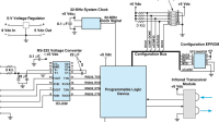
Aerospace & Defense Tech Briefs
Mil-Aero Design Embraces Intelligent Application-Ready ATCA Platforms
Aerospace & Defense Tech Briefs
Evaluation of Four Methods of Reconfiguring an FPGA
Aerospace & Defense Tech Briefs
How Thunderbolt 4 Helps Bring Fault-Tolerant, Distributed Systems to Market

Photonics & Imaging Technology
Rethinking FPGAs for Smart Cameras
Aerospace & Defense Tech Briefs
Rugged Server and Display System
Tech Briefs
Next-Generation Computer Chip Has Two Heads

Tech Briefs
Essential Control and Visualization, Combined
Overview
The document outlines a patent application for a novel method and apparatus designed for networking digital signal processors (DSPs) using field programmable gate arrays (FPGAs). The invention aims to enhance communication between a host DSP and multiple non-host DSPs, facilitating efficient data transmission and processing.
The core of the invention consists of a host DSP that communicates with at least one FPGA. The FPGA serves as an intermediary, receiving digital signals from the host DSP and relaying them to one or more non-host DSPs. This configuration allows for a streamlined communication channel, which is particularly beneficial in complex networking scenarios where multiple DSPs need to operate in concert.
The document includes a brief description of the prior art, highlighting the limitations of existing methods for connecting DSPs. Traditional approaches often involve complex and costly setups, which can hinder performance and scalability. By utilizing FPGAs, the present invention simplifies the architecture, potentially reducing costs and improving the overall efficiency of the network.
Figures included in the document illustrate various configurations of the proposed system. For instance, one figure depicts a network where a host DSP communicates with several non-host DSPs through an FPGA, showcasing the flexibility and scalability of the design. Another figure presents an embodiment that incorporates multiple slave/host DSPs, further emphasizing the versatility of the invention.
The document also mentions the potential applications of this technology, particularly in governmental contexts, as it states that the invention may be manufactured and used by or for the Government of the United States without the payment of royalties. This aspect underscores the invention's relevance to defense and other governmental operations that rely on advanced digital signal processing capabilities.
In summary, the patent application presents a significant advancement in the field of digital signal processing by proposing a method that leverages FPGAs to create a more efficient and cost-effective networking solution for DSPs. This innovation not only addresses the shortcomings of existing technologies but also opens up new possibilities for applications in various sectors, particularly in government and defense.
Top Stories
INSIDERManufacturing & Prototyping
![]() How Airbus is Using w-DED to 3D Print Larger Titanium Airplane Parts
How Airbus is Using w-DED to 3D Print Larger Titanium Airplane Parts
NewsAutomotive
![]() Microvision Aquires Luminar, Plans Relationship Restoration, Multi-industry Push
Microvision Aquires Luminar, Plans Relationship Restoration, Multi-industry Push
INSIDERAerospace
![]() A Next Generation Helmet System for Navy Pilots
A Next Generation Helmet System for Navy Pilots
INSIDERDesign
![]() New Raytheon and Lockheed Martin Agreements Expand Missile Defense Production
New Raytheon and Lockheed Martin Agreements Expand Missile Defense Production
ArticlesAR/AI
![]() CES 2026: Bosch is Ready to Bring AI to Your (Likely ICE-powered) Vehicle
CES 2026: Bosch is Ready to Bring AI to Your (Likely ICE-powered) Vehicle
Road ReadyDesign
Webcasts
Semiconductors & ICs
![]() Advantages of Smart Power Distribution Unit Design for Automotive...
Advantages of Smart Power Distribution Unit Design for Automotive...
Unmanned Systems
![]() Quiet, Please: NVH Improvement Opportunities in the Early Design...
Quiet, Please: NVH Improvement Opportunities in the Early Design...
Electronics & Computers
![]() Cooling a New Generation of Aerospace and Defense Embedded...
Cooling a New Generation of Aerospace and Defense Embedded...
Power
![]() Battery Abuse Testing: Pushing to Failure
Battery Abuse Testing: Pushing to Failure
AR/AI
![]() A FREE Two-Day Event Dedicated to Connected Mobility
A FREE Two-Day Event Dedicated to Connected Mobility