


Assembly of Nanowire-Based Computing Systems
Ultra-high densities would enable processing and memory power to reach unprecedented levels.
A program to develop ultra-dense integrated digital data-processing systems and circuits based on nanowires involves utilization of hybrid top-down and bottom-up assembly techniques to implement designs representative of a highly reliable defect- and fault-tolerant architecture. This program has included fabrication and assembly of molecular- scale logic blocks based on arrays of overlapping semiconducting nanowires, using novel wafer-scale assembly techniques. On the basis of breakthrough addressing techniques, these logic blocks have been connected to ultradense memory blocks and to external complementary oxide/semiconductor (CMOS)-process lithographic interfaces for testing. One of the main underlying ideas is to construct highly reliable components out of high-defect-density logic and memory elements, using recently developed sublithographic-scale programmable- logic-array architectures that incorporate novel reliable-circuit concepts and higher-level redundancy mechanisms. Using state-of-the-art modeling techniques and computational simulations, test designs have been optimized, various defect-tolerance approaches have been developed, and development and optimization of larger systems are continuing.
The accomplishments of this program thus far include the following:
Demonstration of Basic Logic Structures Without Feedback for Two-Bit Words
- A two-bit adder consisting of AND1/ inverter/AND2 stages was designed and simulated.
- It was demonstrated that two-bit adder structures could be consistently fabricated following a hybrid assembly-andlithography- based approach.
- Basic properties and statistics of device elements were characterized.
- Two-bit adder structures were assembled and validated by demonstrating them to be capable of performing an essential product-of-sums function.
Demonstration of Local Device Pitch of ≈ 100 nm
- It was shown that following the assembly- and-lithography approach, one can fabricate reliably crossed arrays of nanowires for logic circuits having local device pitches of the order of 100 nm. Demonstration of Two to Five Logic Tiles on One Die
- Hybrid assembly and lithography were demonstrated for fabrication of two or more logic tiles per standard die or chip, using a scalable process that is readily extensible to fabrication of devices for performing more-complex logic and computation.
Demonstration of State-of-the-Art Nanowire Devices
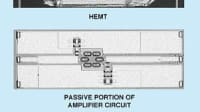
- A core/shell germanium/silicon nanowire heterostructure transistor having scaled performance parameters that exceed those of the best corresponding CMOS transistors by a factor of about 4 was demonstrated.
- A core/shell silicon/barium titanate structure that functions as the first nonvolatile and reversibly switchable nanowire transistor was demonstrated.
Continuation of this program promises to lead to development of computer hardware offering unprecedented levels of processing and memory power. Such hardware could enable satisfaction of requirements for cheap, highly dispersed, sensor-processor-memory communication systems for military applications. After further development, such hardware might be useful for massive direct digital electronic interfaces to nerves, scalable emulation engines, and other applications yet to be imagined.
This work was done by Charles M. Lieber of Harvard University for the Air Force Research Laboratory. For further information, download the free white paper at www.defensetechbriefs.com under the Electronics/Computers category. AFRL-0013
This Brief includes a Technical Support Package (TSP).

Assembly of Nanowire-Based Computing Systems
(reference AFRL-0013) is currently available for download from the TSP library.
Don't have an account?
More From SAE Media Group
Tech Briefs
Thin-Film Electronics for Flexible Chip Design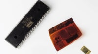
Tech Briefs
A Two-in-One Storage and Computing Device

Aerospace & Defense Tech Briefs
Heterogeneous Integration Technology

Tech Briefs
Next-Generation Computer Chip Has Two Heads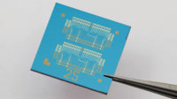
Electronics & Sensors INSIDER
Integrating Dimensions to Get More Out of Moore’s Law
Electronics & Sensors INSIDER
Opening Up the Potential of Thin-Film Electronics for Flexible Chip Design

Embedded Technology
The Physics of Failure: Predicting Reliability in Electronic Components
Electronics & Sensors INSIDER
Engineers “Grow” Atomically Thin Transistors on Top of Computer Chips
Aerospace & Defense Tech Briefs
Magnetic Memory Devices for Embedded Computing
Tech Briefs
5Ws of the Silk Transistor
Electronics & Sensors INSIDER
Brain-Inspired Highly Scalable Neuromorphic Hardware
Tech Briefs
Graphene “Nano-Origami” Creates Tiny Microchips

Tech Briefs
Reconfigurable Chaos-Based Microchips
Electronics & Sensors INSIDER
MIT Engineers Grow “High-Rise” 3D Chips
Electronics & Sensors INSIDER
Advancing Semiconductor Devices for Artificial Intelligence
Tech Briefs
Single Event Upset Suppression System (SEUSS)
Electronics & Sensors INSIDER
A Ferroelectric Transistor That Stores and Computes at Scale
Embedded Computing INSIDER
High-Efficiency Power Amplifier Could Bring 5G Cell Phones


Tech Briefs
SEU-Tolerant Flip-Flops
Photonics & Imaging Technology
Sustainable Computing for AI Processing

Overview
The document is a final technical report detailing the progress and achievements of a research program focused on the assembly of ultra-dense nanowire-based computing systems, covering the period from July 1, 2005, to March 31, 2006. Authored by Charles M. Lieber and sponsored by the Air Force Office for Scientific Research, the report outlines significant advancements in the field of nanoscale electronic devices.
The executive summary emphasizes the challenges of developing effective integrated digital information processing systems, which require innovative assembly techniques that are both defect- and fault-tolerant. The report highlights the potential of semiconducting nanowires (NWs) in creating high-performance field-effect transistors (FETs). It discusses the limitations posed by traditional metal contacts, which often create Schottky barriers that hinder device performance. In contrast, the research team successfully demonstrated the use of transparent contacts and low bias ballistic transport in undoped germanium/silicon core/shell NW heterostructures, achieving an estimated scattering mean free path of approximately 500 nm.
The report also details the fabrication of devices utilizing high-k gate dielectrics, such as hafnium oxide (HfO2) and zirconium oxide (ZrO2), which enhance the performance of the nanowire transistors. The findings indicate that the unique properties of Ge/Si NW heterostructures can lead to improved performance due to reduced scattering and a limited number of conduction channels.
In addition to the scientific results, the report outlines the methodologies employed in the research, including novel wafer-scale assembly techniques for creating overlapping semiconducting nanowire arrays. These techniques enable the construction of complex molecular logic elements that can be integrated with ultra-dense memory blocks and connected to external CMOS lithographic interfaces for testing.
Overall, the report presents a comprehensive overview of the advancements made in nanowire-based computing systems, showcasing the potential for these technologies to meet the aggressive goals set forth by the MoleComputing program. The research not only contributes to the understanding of thermal transport phenomena in nanowires but also paves the way for the development of minimal energy dissipative devices, which are critical for future electronic applications.
Top Stories
INSIDERManufacturing & Prototyping
![]() How Airbus is Using w-DED to 3D Print Larger Titanium Airplane Parts
How Airbus is Using w-DED to 3D Print Larger Titanium Airplane Parts
NewsAutomotive
![]() Microvision Aquires Luminar, Plans Relationship Restoration, Multi-industry Push
Microvision Aquires Luminar, Plans Relationship Restoration, Multi-industry Push
INSIDERAerospace
![]() A Next Generation Helmet System for Navy Pilots
A Next Generation Helmet System for Navy Pilots
INSIDERDesign
![]() New Raytheon and Lockheed Martin Agreements Expand Missile Defense Production
New Raytheon and Lockheed Martin Agreements Expand Missile Defense Production
ArticlesAR/AI
![]() CES 2026: Bosch is Ready to Bring AI to Your (Likely ICE-powered) Vehicle
CES 2026: Bosch is Ready to Bring AI to Your (Likely ICE-powered) Vehicle
Road ReadyDesign
Webcasts
Semiconductors & ICs
![]() Advantages of Smart Power Distribution Unit Design for Automotive...
Advantages of Smart Power Distribution Unit Design for Automotive...
Unmanned Systems
![]() Quiet, Please: NVH Improvement Opportunities in the Early Design...
Quiet, Please: NVH Improvement Opportunities in the Early Design...
Electronics & Computers
![]() Cooling a New Generation of Aerospace and Defense Embedded...
Cooling a New Generation of Aerospace and Defense Embedded...
Power
![]() Battery Abuse Testing: Pushing to Failure
Battery Abuse Testing: Pushing to Failure
AR/AI
![]() A FREE Two-Day Event Dedicated to Connected Mobility
A FREE Two-Day Event Dedicated to Connected Mobility