


Near-Field Light Lenses for Nano-Focusing of Beams of Atoms
Lenses like these could contribute to development of nanodevices in general.
Near-field light lenses for focusing beams of light and beams of atoms to spots having a width of no more than several nanometers are undergoing development. There are numerous potential applications for such lenses:
•A capability to focus beams of light to nanometer-sized spots is essential for development of proposed nanoscale optical devices (e.g., optical switches and logic gates) based on near-field optical interactions.
•A capability to focus beams of atoms to nanometer-sized spots could contribute to the development of nanophotonic devices, including quantum dots, which must be sized and positioned with precision.
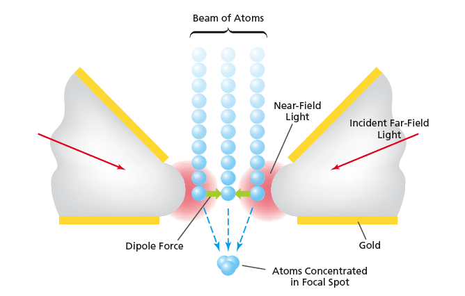
Experimental lenses based on this principle were fabricated on silicon-on-insulator surfaces, using standard techniques of photolithography and etching to form the holes, and vacuum evaporation to apply reflective coats of gold. At the time of reporting the information for this article, the lenses had not yet been tested in operation, but computational simulations of operation under representative conditions had been performed. In these simulations, the spatial distribution of 780-nm-wavelength near-field illumination produced by a lens having a 500-nm-diameter circular cross section exit hole was computed by use of commercial software that solves the applicable equations of electromagnetism by finite-difference time-domain analysis techniques. Then the spatial distribution of the near-field light was used in solving the Schrödinger equation for a Gaussian wave packet of a cold beam of rubidium atoms incident on the hole at an axial velocity of 1 m/s. From the numerical results of the simulation, the full width at half-maximum of the zeroth diffraction pattern of the deBroglie waves of the beam, which width is considered to approximate the width of the focal spot, was estimated to be 2 nm — comparable to the deBroglie wavelength.
This work was done by Haruhiko Ito of Tokyo Institute of Technology for the Air Force Research Laboratory.
AFRL-0081
This Brief includes a Technical Support Package (TSP).
Near-Field Light Lenses for Nano-Focusing of Beams of Atoms
(reference AFRL-0081) is currently available for download from the TSP library.
Don't have an account?
More From SAE Media Group
Photonics & Imaging Technology
How to Innovate and Overcome the Challenges of Blue Laser Beam Shaping

Tech Briefs
Compact Laser Source Detects Pollution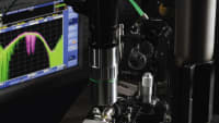
Photonics & Imaging Technology INSIDER
Tying Overlapping Laser Beams into Stable 'Optical Knots'
Aerospace & Defense Tech Briefs
Frequency Agile Plasmonic Antennas and Sensors
Photonics & Imaging Technology
Challenges of Coating Aspheric Lenses
Photonics & Imaging Technology
Meta Optical Elements
Photonics & Imaging Technology
New “Metalens” Shifts Focus Without Tilting or Moving
Photonics & Imaging Technology
SPIE Photonics West 2022 Preview
Photonics & Imaging Technology
SPIE Photonics West 2023 Preview

Photonics & Imaging Technology
Photonics West 2021 Preview
Tech Briefs
New Family of Glass for Lens Applications

Photonics & Imaging Technology
Overcoming the Optical Resolution Limit
Photonics & Imaging Technology
Lunar Lens: First Compact Flat Metalens Images Moon Surface

Tech Briefs
Completely Flat Fisheye Lens
Photonics & Imaging Technology INSIDER
Tiny Diamond Mirrors Could Smooth Out Already Revolutionary X-Ray Lasers
Photonics Tech Briefs
Improved Cross-Correlation Dynamic-Light-Scattering Method

Photonics & Imaging Technology
A First-Of-Its-Kind Integrated Optical Isolator
Photonics & Imaging Technology
Micro Molding and Micro-Optics
Air Force Research Laboratory Technology Horizons
Surface-Emitting Laser Arrays Bring Light to the Top
Photonics & Imaging Technology INSIDER
Infrared Imaging by Ultrathin Nanocrystal Layers
Photonics & Imaging Technology
Making Measurements with a Fine-Toothed Comb
Photonics & Imaging Technology
Optical Signal Amplifying Technique
Aerospace & Defense Tech Briefs
On the Pulsed Laser Ablation of Metals and Semiconductors
Overview
The document presents a final report on the development of a near-field-light lens aimed at focusing rubidium (Rb) atoms into nanometer-sized spots. Conducted by Haruhiko Ito and his team at the Tokyo Institute of Technology, the research focuses on the fabrication and application of nanophotonic devices that leverage near-field optical interactions.
The primary goal of the project was to create a system capable of concentrating atoms using localized near-field light, which is generated near the edge of a small hole in a specially designed lens structure. The lens is fabricated from a silicon-on-insulator (SOI) wafer, consisting of multiple layers, including a 3-μm-thick SiO2 layer and two silicon layers of varying thicknesses. The fabrication process involves several steps, including photolithography and chemical etching, to create a hollow inverse pyramidal structure that serves as the atom lens.
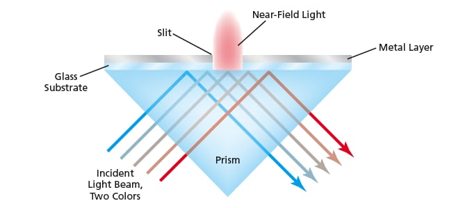
The report details the design of the lens, which features a small exit hole that can be shaped either rectangularly or circularly, with the latter being preferred for homogeneous focusing. The circular hole, with a diameter of 500 nm and a radius of curvature of approximately 45 nm, is etched using a specific chemical solution. The near-field light produced at this exit hole is crucial for the atom concentration process.
Simulations were conducted to assess the feasibility of nanofocusing, revealing the light intensity distribution within the 500-nm hole when illuminated with a wavelength of 780 nm, suitable for Rb atoms. The report also discusses the principles of atom focusing, which relies on the repulsive dipole forces generated by blue-detuned near-field light, effectively concentrating atoms into a nanometer-scale spot.
Additionally, the researchers fabricated a nano-slit to detect the focused atoms and estimated the detection efficiency of Rb atoms numerically. The findings indicate significant potential for the application of these near-field optical devices in quantum technology, including optical switches and logic gates, which require precise control at the nanoscale.
Overall, this research contributes to the advancement of nanophotonics and the development of devices that can manipulate atomic-scale interactions, paving the way for future innovations in the field.
Top Stories
NewsRF & Microwave Electronics
![]() Microvision Aquires Luminar, Plans Relationship Restoration, Multi-industry Push
Microvision Aquires Luminar, Plans Relationship Restoration, Multi-industry Push
INSIDERAerospace
![]() A Next Generation Helmet System for Navy Pilots
A Next Generation Helmet System for Navy Pilots
INSIDERDesign
![]() New Raytheon and Lockheed Martin Agreements Expand Missile Defense Production
New Raytheon and Lockheed Martin Agreements Expand Missile Defense Production
INSIDERMaterials
![]() How Airbus is Using w-DED to 3D Print Larger Titanium Airplane Parts
How Airbus is Using w-DED to 3D Print Larger Titanium Airplane Parts
NewsPower
![]() Ford Announces 48-Volt Architecture for Future Electric Truck
Ford Announces 48-Volt Architecture for Future Electric Truck
ArticlesAR/AI
Webcasts
Electronics & Computers
![]() Cooling a New Generation of Aerospace and Defense Embedded...
Cooling a New Generation of Aerospace and Defense Embedded...
Automotive
![]() Battery Abuse Testing: Pushing to Failure
Battery Abuse Testing: Pushing to Failure
Power
![]() A FREE Two-Day Event Dedicated to Connected Mobility
A FREE Two-Day Event Dedicated to Connected Mobility
Unmanned Systems
![]() Quiet, Please: NVH Improvement Opportunities in the Early Design Cycle
Quiet, Please: NVH Improvement Opportunities in the Early Design Cycle
Automotive
![]() Advantages of Smart Power Distribution Unit Design for Automotive &...
Advantages of Smart Power Distribution Unit Design for Automotive &...
Energy
![]() Sesame Solar's Nanogrid Tech Promises Major Gains in Drone Endurance
Sesame Solar's Nanogrid Tech Promises Major Gains in Drone Endurance