


Photonic-Crystal-Based Devices for Commercial Applications
Waveguides, beam splitters, filters, and routers are implemented in photonic crystals.
Several analog-to-digital converter (ADC) devices and part of a multispectral receiver have been designed, fabricated, and tested to demonstrate their feasibility as part of an effort to establish the organizational and technological foundation for development of photonic-crystal-based devices for commercial and military applications. Also known as photonic-band-gap devices, photonic crystals contain periodic structures having feature sizes in the submicron range — less than the wavelengths of light that the devices are intended to handle. Photonic crystals can be fabricated by techniques used in the integrated-circuit and microelectromechanical systems (MEMS) industries.
The periodic structures can be tailored to manipulate and control light in a wide variety of ways. In an important class of contemplated applications, photonic crystals of predominantly two-dimensional character would be used for in-plane distribution and routing of optical signals, while photonic crystals of three-dimensional character would be used for out-of-plane distribution and routing of optical signals. In both the two- and three-dimensional cases, the photonic crystals would make it possible to provide high-density optical interconnections among multiple photonic and/or optoelectronic circuits oriented at various angles to the photonic crystals.
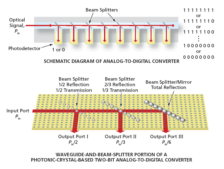
The basic principle of an ADC of the present type is illustrated in the upper part of Figure 1. A cascade of beam splitters at various positions along a waveguide apportions the power of an incoming optical signal (Pin) into multiple channels by specific fractions that correspond to a specific digital (typically, binary) representation of the signal power. In each channel, there is a photodetector. Relying on the nonlinear response of the photodetector, a signal is deemed to be present or not present in the channel depending on whether the signal power is above or below, respectively, a threshold power (Pth) for that photodetector. A relatively strong signal has enough power to be detected in all the channels along the cascade. As the signal strength is reduced, the power progressively falls below threshold at the most distant detectors. Thus, as the signal power decreases, the digital representation of the signal power changes as depicted on the right side of the upper part of Figure 1.
The lower part of Figure 1 depicts the layout of the waveguide-and-beam-splitting portion of a two-bit ADC of this type based on a two-dimensional photonic-crystal/waveguide structure. The splitting ratios shown in the figure are chosen in consideration of the nonlinear photodetector response. When Pin < 2Pth, the output powers at all three output ports are <Pth and, consequently, the quantized state of the photodetector outputs at the three output ports is hence defined as “000.” When the input power is slightly above 2Pth, the output power at port I only is slightly above threshold, making the quantized state “100.” Similarly, as Pin increases, causing the power levels at the other output ports to rise above Pth, their quantized states change from “0” to “1.” The net result is that as Pin increases past integer multiples of Pth, the quantized states exhibit the sequence “000,” “100,” “110,” and “111.” These four states can be coded into the states “00”, “01”, “10”, and “11” of a two-bit ADC.
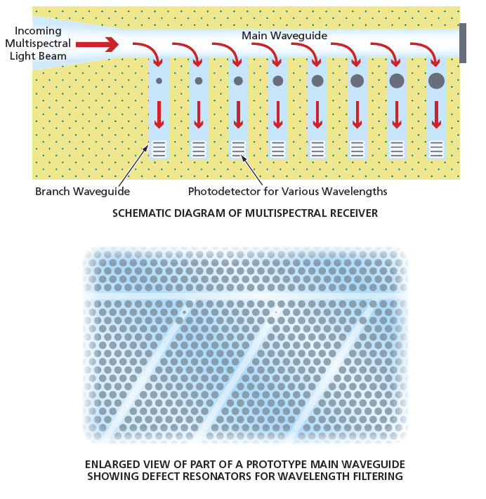
Figure 2 illustrates the principle of operation of a photonic-crystal-based multispectral receiver, part of which has been built and tested. A multispectral infrared beam is launched into a two-dimensional main photonicband- gap waveguide that supports propagation at the wavelengths of interest. The waveguide is implemented as a periodic array of holes in a silicon-on-insulator chip. Resonators, implemented as localized defects in the photonic-crystal structure of the waveguide, are used for filtering light of individual wavelengths of interest into branch waveguides that, in a fully developed version, would lead to photodetectors. Proposed further developments include integration of a photonic-crystal-based multispectral receiver with ADCs and an optical switching network.
This work was done by Ahmed Sharkawy, Shouyuan Shi, and Caihua Chen of EM Photonics, Inc.; and Dennis Prather of the University of Delaware for the Air Force Research Laboratory. For more information, download the Technical Support Package (free white paper) at www.defensetechbriefs.com/tsp under the Photonics category. AFRL-0007
This Brief includes a Technical Support Package (TSP).
Photonic-Crystal-Based Devices for Commercial Applications
(reference AFRL-0007) is currently available for download from the TSP library.
Don't have an account?
More From SAE Media Group

Tech Briefs
Serial Arrayed Waveguide Grating
Photonics & Imaging Technology
A First-Of-Its-Kind Integrated Optical Isolator
Aerospace & Defense Tech Briefs
High-Power Broadband Multispectral Source on a Hybrid Silicon Chip
Photonics Tech Briefs
Silicon Modulator Brings Optical Computing A Step Closer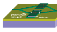
Aerospace & Defense Tech Briefs
Frequency Agile Plasmonic Antennas and Sensors
Aerospace & Defense Tech Briefs
Ultracompact, High-Speed Field-Effect Optical Modulators
Photonics & Imaging Technology
New Device Modulates Visible Light with the Smallest Footprint and Lowest Power Consumption
Photonics & Imaging Technology
Researchers Create World’s Smallest LED And Holographic Microscope
Photonics & Imaging Technology
Ultra-Broadband Photonic Chip Boosts Optical Signals
Photonics & Imaging Technology
Optical Signal Amplifying Technique
Tech Briefs
Programming Light on a Chip
Photonics & Imaging Technology
Moving Precision Communication, Metrology, Quantum Applications from Lab to Chip
Aerospace & Defense Tech Briefs
Photonic Microwave Generation Using On-Chip Optical Frequency Combs

Photonics & Imaging Technology
A Marriage of Light-Manipulation Technologies
Aerospace & Defense Tech Briefs
Photonic Analog-to-Digital Converters
Photonics Tech Briefs
Integrated Miniature Arrays of Optical Biomolecule Detectors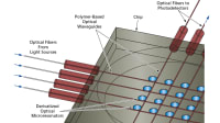
Tech Briefs
Compact Infrared Spectrometer
Sensor Technology
Nano Flashlight Enables New Applications of Light

Photonics & Imaging Technology
Using Magnets to Toggle Nanolasers Leads to Better Photonics
Photonics & Imaging Technology
Novel Light-Field Sensor for 3D Scene Construction Has Unprecedented Angular Resolution
Photonics & Imaging Technology
Photonic Integrated Circuit Testing: Accelerating R&D From Lab to Fab
Photonics & Imaging Technology
Overcoming Pitfalls When Measuring Thin, Parallel Optics
Tech Briefs
Twisted Moiré Photonic Crystals
Photonics & Imaging Technology
Sensitive Yet Tough Photonic Devices Are Now a Reality
Photonics & Imaging Technology
A Laser That Could Reshape the Landscape of Integrated Photonics
Aerospace & Defense Tech Briefs
Low Power Optical Phase Array Using Graphene on Silicon Photonics
Overview
The document is a final report on the development of Photonic Bandgap (PBG) devices for commercial applications, prepared by EM Photonics under AFOSR Contract # FA9550-04-C-0062. The primary objective of the project was to establish a unified manufacturing process that integrates design, simulation, fabrication, and testing of PBG devices, which are crucial for advancing nanophotonic technologies.
The report outlines a three-tiered approach to achieve the project's goals: first, establishing close collaborations with two Air Force Research Laboratory (AFRL) teams to align research efforts with military needs; second, identifying and demonstrating the feasibility of suitable nanophotonic devices for rapid commercialization; and third, exploring innovative devices and fabrication processes for next-generation PBG technologies.
Key achievements highlighted in the report include successful collaborations with AFRL researchers, which facilitated the integration of PBG devices into existing Air Force research programs. The document emphasizes the importance of developing high-resolution templates and methodologies for acid transfer, as well as controlling environmental conditions to ensure the fidelity of patterns during fabrication.
The report also discusses the competitive landscape, acknowledging existing companies like Molecular Imprints and others in the nanotechnology sector. EM Photonics aims to differentiate itself through its unique technology, which is designed to be smaller, less invasive, and adaptable for both high and low-volume production.
Intellectual property protection is identified as a critical asset for EM Photonics, with a patent disclosure process established early in the company's inception. The report notes that several disclosures have been filed, and all employees and contractors are required to sign non-disclosure and non-compete agreements to safeguard proprietary information.
In terms of marketing strategy, the company focuses on presenting research at key scientific conferences, maintaining a customer database, and keeping an updated website to attract potential customers and collaborators. The report concludes with a call for continued collaboration and commercialization efforts in the field of nanophotonics, emphasizing the potential impact of PBG devices on various applications, including telecommunications, sensing, and advanced manufacturing.
Overall, the document serves as a comprehensive overview of the project's objectives, methodologies, achievements, and future directions in the realm of photonic technologies.
Top Stories
NewsRF & Microwave Electronics
![]() Microvision Aquires Luminar, Plans Relationship Restoration, Multi-industry Push
Microvision Aquires Luminar, Plans Relationship Restoration, Multi-industry Push
INSIDERAerospace
![]() A Next Generation Helmet System for Navy Pilots
A Next Generation Helmet System for Navy Pilots
INSIDERDesign
![]() New Raytheon and Lockheed Martin Agreements Expand Missile Defense Production
New Raytheon and Lockheed Martin Agreements Expand Missile Defense Production
INSIDERMaterials
![]() How Airbus is Using w-DED to 3D Print Larger Titanium Airplane Parts
How Airbus is Using w-DED to 3D Print Larger Titanium Airplane Parts
NewsPower
![]() Ford Announces 48-Volt Architecture for Future Electric Truck
Ford Announces 48-Volt Architecture for Future Electric Truck
ArticlesAR/AI
Webcasts
Electronics & Computers
![]() Cooling a New Generation of Aerospace and Defense Embedded...
Cooling a New Generation of Aerospace and Defense Embedded...
Automotive
![]() Battery Abuse Testing: Pushing to Failure
Battery Abuse Testing: Pushing to Failure
Power
![]() A FREE Two-Day Event Dedicated to Connected Mobility
A FREE Two-Day Event Dedicated to Connected Mobility
Unmanned Systems
![]() Quiet, Please: NVH Improvement Opportunities in the Early Design Cycle
Quiet, Please: NVH Improvement Opportunities in the Early Design Cycle
Automotive
![]() Advantages of Smart Power Distribution Unit Design for Automotive &...
Advantages of Smart Power Distribution Unit Design for Automotive &...
Energy
![]() Sesame Solar's Nanogrid Tech Promises Major Gains in Drone Endurance
Sesame Solar's Nanogrid Tech Promises Major Gains in Drone Endurance