


Adaptive Optoelectronic Eyes
Designs of "smart" cameras would be inspired by biological vision systems.
Aprogram of research has built a technological foundation for further development of systems that could be characterized, variously, as "smart" cameras or adaptive optoelectronic eyes. A system according to this concept would function in an optimal manner to capture images under a variety of lighting conditions and would be capable of semi-autonomous recognition of objects.
The approach taken in this research was to combine advances in understanding of the mechanisms of biological vision systems with advances in hybrid electronic/photonic packaging technology in order to develop algorithms, architectures, and optical and electronic hardware components and subsystems essential to building artificial, biologically inspired vision systems.
A primary goal of this research was to enable the development of a sensor/processor module (1) in which the sensor and processor would be intimately coupled and (2) that would have architectural characteristics and capabilities similar to those of the multilayer retina and early stages of vision in a mammalian visual system. The module would be a compact, multilayer, vertically integrated structure, containing very-large-scale integrated (VLSI) circuit chips. It would perform both sensing (image-acquisition) and processing functions (for purposes of extraction of features and recognition of objects, for example).
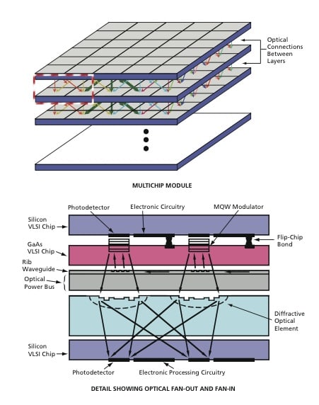
The lower part of the figure presents an enlarged view of the portion highlighted by the rectangle in the upper part of the figure, showing an example of dense optical fan-out/fan-in interconnections between layers in the multichip module. Each pixel of the lower silicon VLSI chip would contain both processing electronic circuitry and a photodetector illuminated with image-bearing or other information from the layer above it. An array of multiple-quantum-well (MQW) modulators is shown to be flipchip bonded to the silicon pixel array. An optical power bus (an integrated optical component) would deliver a readout beam to each modulator element in the array by means of an array of rib waveguides containing vertical-outcoupling gratings. Each diffractive optical element would provide weighted fanout connections from the modulator element of the corresponding pixel in the upper VLSI chip to the photodetectors of several neighboring pixels on the lower silicon VLSI chip.
This work was done by Armand R. Tanguay Jr., B. Keith Jenkins, Christoph von der Malsburg, Bartlett Mel, Irving Biederman, John O'Brien, and Anupam Madhukar of the University of Southern California for the Army Research Laboratory. For more information, download the Technical Support Package (free white paper) at www.defensetechbriefs.com/tsp under the Photonics category. ARL-0013
This Brief includes a Technical Support Package (TSP).

Adaptive Optoelectronic Eyes
(reference ARL-0013) is currently available for download from the TSP library.
Don't have an account?
More From SAE Media Group
Photonics & Imaging Technology
Photonic Integrated Circuit Testing: Accelerating R&D From Lab to Fab
Tech Briefs
Ultra-Thin Sensor for Smart Contact Lenses
Photonics & Imaging Technology
Optical Modules
Photonics & Imaging Technology
A Technological Breakthrough for Ultra-Fast and Greener AI
Photonics & Imaging Technology INSIDER
STARLight Project Launches European Value Chain for Silicon Photonics Production
Power Electronics INSIDER
Powerful and Precise Multi-color Lasers Now Fit on a Single Chip
Photonics & Imaging Technology
Why Honda Wants FMCW LiDAR in Next Generation Mobility
Tech Briefs
Compact 3D LiDAR Imaging System
Photonics & Imaging Technology
Thermal Imaging — Making Hidden Details Visible
Aerospace & Defense Tech Briefs
Photonic Analog-to-Digital Converters
Photonics & Imaging Technology
Researchers Create World’s Smallest LED And Holographic Microscope
Photonics & Imaging Technology
A First-Of-Its-Kind Integrated Optical Isolator
Photonics Tech Briefs
Optoelectronic Contract Manufacturing Starts Before Design — Not After
Photonics & Imaging Technology
Backside Illumination Gets Fast
Photonics & Imaging Technology INSIDER
Photonics West 2024: 5 New Technologies on Display This Year

Photonics & Imaging Technology INSIDER
Can Lithium Tantalate Lower the Cost of Manufacturing Photonic Integrated Circuits?
Photonics Tech Briefs
Curved Focal-Plane Arrays Using Back-Illuminated High-Purity Photodetectors
Photonics & Imaging Technology
Integrated Silicon Photonic Switch Demonstrates Lowest Signal Loss Ever in High-Speed Data Transmission

Photonics Tech Briefs
Beyond Smart Vision
Aerospace & Defense Tech Briefs
BC VCSELs for RF/Photonic Links
Photonics Tech Briefs
Active Fiber Optic Microelectromechanical Systems Aligner
Photonics & Imaging Technology
Sensitive Yet Tough Photonic Devices Are Now a Reality
Photonics & Imaging Technology
Sustainable Computing for AI Processing
Photonics & Imaging Technology
New Products
Aerospace & Defense Tech Briefs
Researchers Demonstrate the First Chip-Based 3D Printer
Photonics & Imaging Technology
Wavelength-Multiplexed Diffractive Optical Processor Computes Hundreds of Linear Transformations in Parallel
Photonics & Imaging Technology
Light-Analyzing ‘Lab on A Chip’ Opens Door to Widespread Use of Portable Spectrometers
Photonics Tech Briefs
Downsampling Photodetector Array With Windowing
Overview
The document is the final progress report for the research program titled "Adaptive Optoelectronic Eyes: Hybrid Sensor/Processor Architectures," which was conducted from June 1, 1998, to May 31, 2004, under the Multidisciplinary Research Program of the University Research Initiative. The program aimed to develop advanced vision systems that mimic the biological processes of mammalian vision, focusing on the integration of sensor and processor technologies in a compact, hybrid electronic/photonic multichip module.
The report outlines significant accomplishments in two main areas: vision algorithms and models, and hybrid electronic/photonic hardware implementations. A key objective was to create a tightly coupled sensor/processor module that emulates the multilayer structure of the retina, facilitating efficient image acquisition and processing. The research explored various vision algorithms, including object recognition systems that utilize features inspired by mammalian vision, such as Gabor wavelets. This approach allowed for high accuracy in recognizing diverse objects in realistic environments.
The document details the development of an invariant object recognition system, emphasizing the importance of robustness in recognizing objects despite variations in pose, scale, and depth. The research also included the extraction of shape-defining contours and the analysis of trade-offs in visual representations, contributing to a deeper understanding of feature learning in vision systems.
Technologically, the program made strides in addressing the challenges of integrating multiple silicon VLSI vision chips into a hybrid architecture. This involved the use of novel diffractive optical structures for efficient interconnections and the characterization of key components like vertical cavity surface-emitting laser arrays (VCSELs) and diffractive optical elements (DOEs). The report highlights the interactions between vision algorithms and hardware implementations, which were crucial for the program's success.
Despite the innovative advancements, the report notes that no patent applications were filed during the research period. However, there were significant interactions with Department of Defense agencies and corporations, indicating early stages of technology transfer for the research outcomes.
Overall, the report encapsulates a multidisciplinary effort to advance the field of vision systems through the integration of biological principles, innovative algorithms, and cutting-edge hardware technologies, paving the way for future developments in adaptive optoelectronic eyes.
Top Stories
INSIDERManufacturing & Prototyping
![]() How Airbus is Using w-DED to 3D Print Larger Titanium Airplane Parts
How Airbus is Using w-DED to 3D Print Larger Titanium Airplane Parts
INSIDERManned Systems
![]() FAA to Replace Aging Network of Ground-Based Radars
FAA to Replace Aging Network of Ground-Based Radars
NewsTransportation
![]() CES 2026: Bosch is Ready to Bring AI to Your (Likely ICE-powered) Vehicle
CES 2026: Bosch is Ready to Bring AI to Your (Likely ICE-powered) Vehicle
NewsSoftware
![]() Accelerating Down the Road to Autonomy
Accelerating Down the Road to Autonomy
EditorialDesign
![]() DarkSky One Wants to Make the World a Darker Place
DarkSky One Wants to Make the World a Darker Place
INSIDERMaterials
![]() Can This Self-Healing Composite Make Airplane and Spacecraft Components Last...
Can This Self-Healing Composite Make Airplane and Spacecraft Components Last...
Webcasts
Defense
![]() How Sift's Unified Observability Platform Accelerates Drone Innovation
How Sift's Unified Observability Platform Accelerates Drone Innovation
Automotive
![]() E/E Architecture Redefined: Building Smarter, Safer, and Scalable...
E/E Architecture Redefined: Building Smarter, Safer, and Scalable...
Power
![]() Hydrogen Engines Are Heating Up for Heavy Duty
Hydrogen Engines Are Heating Up for Heavy Duty
Electronics & Computers
![]() Advantages of Smart Power Distribution Unit Design for Automotive...
Advantages of Smart Power Distribution Unit Design for Automotive...
Unmanned Systems
![]() Quiet, Please: NVH Improvement Opportunities in the Early Design...
Quiet, Please: NVH Improvement Opportunities in the Early Design...