


Adaptive Quantum Design of Semiconductor Devices
Quantum-physical models and search algorithms are used to find optimal designs.
The term "adaptive quantum design" denotes a methodology for systematically seeking robust, manufacturable designs of semiconductor devices — especially semiconductor optoelectronic devices having nanoscale or even atomic- scale features. This methodology has been developed to complement advances in fabrication capabilities that make it possible to tailor semiconductor devices ever more precisely, such that it likely will soon be possible to routinely control the positions of features as small as atoms and molecules within devices. Because the number of atom configurations that could, potentially, be fabricated is almost unimaginably large and quantum fluctuations and collective quantum phenomena become important at molecular and atomic scales, traditional design methods and traditional models of device physics based on classical physics and semiclassical approximations of quantum phenomena are not adequate for exploration of the vast space of design options.
Accordingly, in adaptive quantum design, the optimal-design problem is solved by means of computational searches to numerically identify the best broken-symmetry spatial configuration of atoms and molecules that produces the best approximation of the objective function. The two major ingredients of adaptive quantum design are a model representing the quantum device physics and an algorithm (e.g. a genetic algorithm) that searches the space of parameters representing the various configurations.
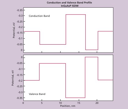
In a study, this methodology was applied in the design of InxGa1-AsyP1-y devices containing broken-symmetry quantum wells (see figure) optimized for excitonic absorption. [In excitonic absorption, excitons (hole/electron pairs somewhat analogous to hydrogen atoms) are formed by absorption of photons of less than the bandgap energy in a direct-bandgap semiconductor. The binding energy of an exciton can be increased by confining the electron and the hole within a two-dimensional quantum well, causing the absorption spectrum to include a strong peak just below the bandgap energy; this fact has been exploited for use in such modern optoelectronic devices as modulators and detectors.] The study included design and fabrication of an electro-absorption modulator. In a test at a wavelength of 1,545 nm, the device was found to perform comparably to the best in a commercial product line of modulators. Further improvements in device performance could be achieved through attention to radio-frequency aspects of the design, which were omitted from the study to enable concentration on demonstrating the basic nature of adaptive quantum design.
This work was done by A. F. J. Levi of the University of Southern California for the Defense Advanced Research Projects Agency (DARPA). For more information, download the Technical Support Package (free white paper) at www.defensetechbriefs.com/tsp under the Electronics/Computers category. DARPA-0002
This Brief includes a Technical Support Package (TSP).

Adaptive Quantum Design of Semiconductor Devices
(reference DARPA-0002) is currently available for download from the TSP library.
Don't have an account?
More From SAE Media Group
Tech Briefs
Turning Thermal Energy into Electricity
Tech Briefs
Quantum Error Correction Method
Photonics & Imaging Technology
Military Optics Technology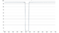
Tech Briefs
Material Increases Efficiency of LED Devices
Aerospace & Defense Tech Briefs
Design Guidelines for Military and Aerospace PCBs
Tech Briefs
Wearable Air Conditioning
Aerospace & Defense Tech Briefs
Testing EMI Materials for Battlefield Applications
Tech Briefs
Turning Diamond into Metal

Electronics & Sensors INSIDER
Scientists Have Visualized the Electronic Structure in a Microelectronic Device
Tech Briefs
University of Colorado Boulder
Electronics & Sensors INSIDER
A New Material That Could Change Electronics
Electronics & Sensors INSIDER
Scientists Create Superconducting Semiconductor Material
Aerospace & Defense Tech Briefs
Creating a Digital Gateway for RF Domain Will Advance Designs That Meet DoD Initiatives
Aerospace & Defense Tech Briefs
Shielding Aerospace Systems from Electromagnetic Interference
Electronics & Sensors INSIDER
Researchers Create First Functional Semiconductor Made from Graphene

Aerospace & Defense Tech Briefs
The US Army’s New AI Supercomputer
Aerospace & Defense Tech Briefs
Transforming Battlespace Communications
Tech Briefs
Superlattice for Sustainable Quantum Electronics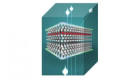
Power Electronics INSIDER
Ultrathin Solar Cells Get a Boost
Aerospace & Defense Tech Briefs
Pathfinder Radar ISR and SAR Systems: Tactical Eyes for the Warfighter
Aerospace & Defense Tech Briefs
A Focal Plane Array and Electronics Model for CMOS and CCD Sensors in the AFIT Sensor and Scene Emulation Tool
Aerospace & Defense Tech Briefs
Ruggedization of Electronics for Deployed Military Environments
Aerospace & Defense Tech Briefs
MOSA Enclosure Design for Military Systems
Aerospace & Defense Tech Briefs
What is Pulse Shaping?
Aerospace & Defense Tech Briefs
Designing Transportable, High-Performance AI Systems for the Rugged Edge
Aerospace & Defense Tech Briefs
Security IP Module
Aerospace & Defense Tech Briefs
Engineered Solutions for Enclosure Sealing and Insulation
Overview
The "Semiconductor Device Synthesis Final Technical Report" presents a comprehensive exploration of the design and synthesis of optoelectronic semiconductor devices, emphasizing a systematic approach to achieving optimal performance. The report highlights the use of modern computational power, adaptive algorithms, and realistic physical models to create robust and manufacturable designs that meet challenging system specifications.
A key focus of the report is the adaptive design of excitonic absorption in broken-symmetry quantum wells, which serves as a prototype system for investigating device synthesis methods. The document discusses the development of a device model that captures essential exciton absorption physics, although it notes that the model does not incorporate radio frequency (RF) design aspects.
Experimental investigations into electro-absorption modulator designs are a significant part of the report. One notable achievement is the measurement of a modulator with a 25 GHz small signal -3 dB response near a wavelength of 1550 nm. This performance is comparable to the best commercially available modulators, such as those from Oki Electric. The report suggests that further enhancements in device performance could be realized by integrating improved RF design elements, particularly through the incorporation of traveling wave electrodes.
The report is structured to provide a clear overview of the research, beginning with an abstract and followed by a table of contents, results, and discussions. It emphasizes the importance of combining theoretical models with practical experimentation to push the boundaries of semiconductor device capabilities.
In summary, this report serves as a valuable resource for researchers and engineers in the field of semiconductor technology, offering insights into the synthesis and design of devices that leverage advanced materials and innovative design strategies. The findings and methodologies discussed could pave the way for future advancements in optoelectronic devices, contributing to the ongoing evolution of technology in this critical area.
Top Stories
NewsRF & Microwave Electronics
![]() Microvision Aquires Luminar, Plans Relationship Restoration, Multi-industry Push
Microvision Aquires Luminar, Plans Relationship Restoration, Multi-industry Push
INSIDERAerospace
![]() A Next Generation Helmet System for Navy Pilots
A Next Generation Helmet System for Navy Pilots
INSIDERDesign
![]() New Raytheon and Lockheed Martin Agreements Expand Missile Defense Production
New Raytheon and Lockheed Martin Agreements Expand Missile Defense Production
INSIDERMaterials
![]() How Airbus is Using w-DED to 3D Print Larger Titanium Airplane Parts
How Airbus is Using w-DED to 3D Print Larger Titanium Airplane Parts
NewsPower
![]() Ford Announces 48-Volt Architecture for Future Electric Truck
Ford Announces 48-Volt Architecture for Future Electric Truck
ArticlesAR/AI
Webcasts
Aerospace
![]() Cooling a New Generation of Aerospace and Defense Embedded...
Cooling a New Generation of Aerospace and Defense Embedded...
Automotive
![]() Battery Abuse Testing: Pushing to Failure
Battery Abuse Testing: Pushing to Failure
Transportation
![]() A FREE Two-Day Event Dedicated to Connected Mobility
A FREE Two-Day Event Dedicated to Connected Mobility
Unmanned Systems
![]() Quiet, Please: NVH Improvement Opportunities in the Early Design Cycle
Quiet, Please: NVH Improvement Opportunities in the Early Design Cycle
Transportation
![]() Advantages of Smart Power Distribution Unit Design for Automotive &...
Advantages of Smart Power Distribution Unit Design for Automotive &...
Energy
![]() Sesame Solar's Nanogrid Tech Promises Major Gains in Drone Endurance
Sesame Solar's Nanogrid Tech Promises Major Gains in Drone Endurance