


NRL Develops Laser Processing Method to Increase Efficiency of Optoelectronic Devices
Scientists at the U.S. Naval Research Laboratory (NRL) discovered a new method to passivate defects in next generation optical materials to improve optical quality and enable the miniaturization of light emitting diodes and other optical elements.
“From a chemistry standpoint, we have discovered a new photocatalytic reaction using laser light and water molecules, which is new and exciting,” said Saujan Sivaram, Ph.D., lead author of the study. “From a general perspective, this work enables the integration of high quality, optically active, atomically thin material in a variety of applications, such as electronics, electro-catalysts, memory, and quantum computing applications.”
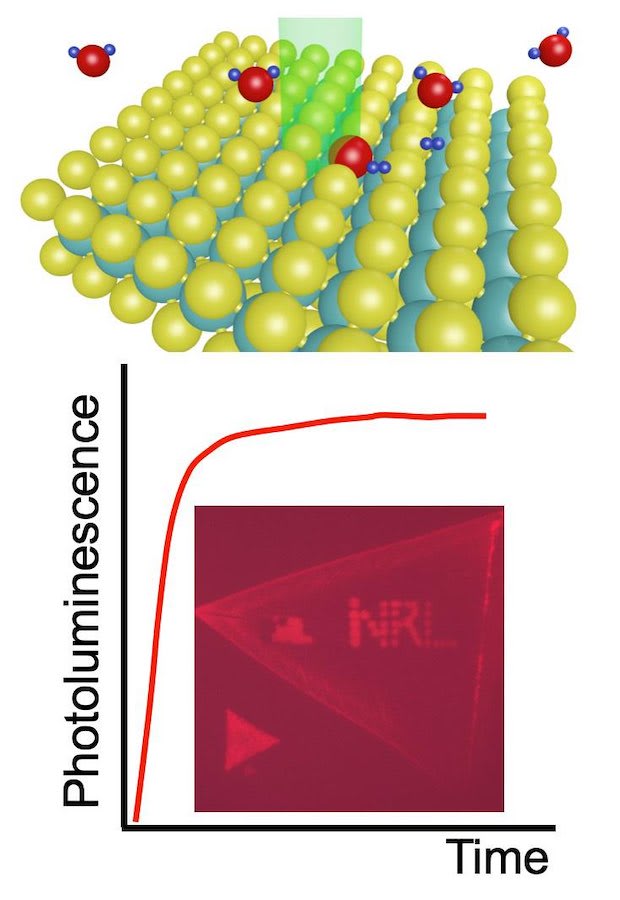
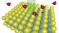
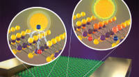
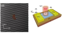
The NRL scientists developed a versatile laser processing technique to significantly improve the optical properties of monolayer molybdenum disulphide (MoS2) — a direct gap semiconductor — with high spatial resolution. Their process produces a 100-fold increase in the material’s optical emission efficiency in the areas “written” with the laser beam. According to Sivaram, atomically thin layers of transition metal dichalcogenides (TMDs), such as MoS2, are promising components for flexible devices, solar cells, and optoelectronic sensors due to their high optical absorption and direct band gap.
“These semiconducting materials are particularly advantageous in applications where weight and flexibility are a premium,” he said. “Unfortunately, their optical properties are often highly variable and non-uniform making it critical to improve and control the optical properties of these TMD materials to realize reliable high efficiency devices.”
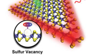
“Defects are often detrimental to the ability of these monolayer semiconductors to emit light,” Sivaram said. “These defects act as non-radiative trap states, producing heat instead of light, therefore, removing or passivating these defects is an important step towards high efficiency optoelectronic devices.”
In a traditional LED, approximately 90 percent of the device is a heat sink to improve cooling. Reduced defects enable smaller devices to consume less power, which results in a longer operational lifetime for distributed sensors and low-power electronics.
The researchers demonstrated that water molecules passivate the MoS2 only when exposed to laser light with an energy above the band gap of the TMD. The result is an increase in photoluminescence with no spectral shift. Treated regions maintain a strong light emission compared to the untreated regions that exhibit much a weaker emission. This suggests that the laser light drives a chemical reaction between the ambient gas molecules and the MoS2.
More From SAE Media Group
Tech Briefs
Material Increases Efficiency of LED Devices
Photonics & Imaging Technology INSIDER
Paving the Way to Electrically Pumped Lasers from Colloidal-Quantum-Dots
Photonics & Imaging Technology
A Sharper Look at the Interior of Semiconductors
Photonics & Imaging Technology
Optimizing Laser Cutting in Semiconductor Advanced Packaging
Photonics & Imaging Technology
How to Innovate and Overcome the Challenges of Blue Laser Beam Shaping

Photonics & Imaging Technology INSIDER
Light from Exotic Crystal Semiconductor Could Lead to Better Solar Cells

Photonics & Imaging Technology
Nanoscale Machines Convert Light into Work


Photonics & Imaging Technology INSIDER
Quantum Dot Breakthrough Could Create Cheaper Infrared Sensors
Tech Briefs INSIDER
Writing with Light: An ‘Etch A Sketch’ Electrical Circuit
Aerospace & Defense Tech Briefs
3D Meta-Optics for High-Energy Lasers
Electronics & Sensors INSIDER
Manufacturing the World's Tiniest Light-Emitting Diodes
Photonics & Imaging Technology
Using Magnets to Toggle Nanolasers Leads to Better Photonics
Photonics & Imaging Technology
Ultrafast Beam-Steering Breakthrough at Sandia Labs
Photonics & Imaging Technology
A First-Of-Its-Kind Integrated Optical Isolator
Tech Briefs
Platform for All-Optical Computing
Photonics & Imaging Technology INSIDER
A Compact, Mid-Infrared Pulse Generator
Tech Briefs
Compact Laser Source Detects Pollution
Photonics & Imaging Technology
Additive Manufacturing of Precision Optics at Micro and Nanoscale
Photonics & Imaging Technology
New Frequency Comb Can Identify Molecules in 20-Nanosecond Snapshots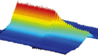
Photonics & Imaging Technology INSIDER
Optics Breakthrough Could Revamp Night Vision
Tech Briefs
5 Ws of Invisible Glass
Top Stories
INSIDERManufacturing & Prototyping
![]() How Airbus is Using w-DED to 3D Print Larger Titanium Airplane Parts
How Airbus is Using w-DED to 3D Print Larger Titanium Airplane Parts
INSIDERManned Systems
![]() FAA to Replace Aging Network of Ground-Based Radars
FAA to Replace Aging Network of Ground-Based Radars
NewsTransportation
![]() CES 2026: Bosch is Ready to Bring AI to Your (Likely ICE-powered) Vehicle
CES 2026: Bosch is Ready to Bring AI to Your (Likely ICE-powered) Vehicle
NewsSoftware
![]() Accelerating Down the Road to Autonomy
Accelerating Down the Road to Autonomy
EditorialDesign
![]() DarkSky One Wants to Make the World a Darker Place
DarkSky One Wants to Make the World a Darker Place
INSIDERMaterials
![]() Can This Self-Healing Composite Make Airplane and Spacecraft Components Last...
Can This Self-Healing Composite Make Airplane and Spacecraft Components Last...
Webcasts
Defense
![]() How Sift's Unified Observability Platform Accelerates Drone Innovation
How Sift's Unified Observability Platform Accelerates Drone Innovation
Automotive
![]() E/E Architecture Redefined: Building Smarter, Safer, and Scalable...
E/E Architecture Redefined: Building Smarter, Safer, and Scalable...
Power
![]() Hydrogen Engines Are Heating Up for Heavy Duty
Hydrogen Engines Are Heating Up for Heavy Duty
Electronics & Computers
![]() Advantages of Smart Power Distribution Unit Design for Automotive...
Advantages of Smart Power Distribution Unit Design for Automotive...
Unmanned Systems
![]() Quiet, Please: NVH Improvement Opportunities in the Early Design...
Quiet, Please: NVH Improvement Opportunities in the Early Design...