


FPGA
Microsemi Corp. (Aliso Viejo, CA) has introduced the SmartFusion®2 system- on-chip (SoC) field programmable gate array (FPGA). SmartFusion2 integrates flash-based FPGA fabric, a 166 megahertz (MHz) ARM® Cortex™-M3 processor, security processing accelerators, DSP blocks, SRAM, eNVM, and communication interfaces on one chip. SmartFusion2 provides a root-of-trust device with secure key storage capability using the physically unclonable function (PUF) key enrollment and regeneration. Users may also leverage built-in cryptographic processing accelerators including: advanced encryption standard (AES) AES-256, secure hash algorithm (SHA) SHA-256, 384 bit elliptical curve cryptographic (ECC) engine, and a non-deterministic random bit generator (NRBG).
 SmartFusion2 devices are available with a range of density from 5K LUT to 120K LUT, plus embedded memory and multiple accumulate blocks for digital signal processing (DSP). High-bandwidth interfaces include PCI Express (PCIe) with flexible 5G SERDES, along with highspeed double data rate DDR2/DDR3 memory controllers. The device also includes a microprocessor sub-system (MSS) with a 166 MHz ARM Cortex-M3 processor, on-chip 64KB eSRAM, and 512KB eNVM.
For Free Info Click Here
More From SAE Media Group
Aerospace & Defense Tech Briefs
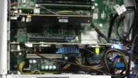
FPGAs and HPC
Aerospace & Defense Tech Briefs
New Products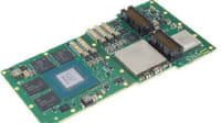
Embedded Technology
Extensible Processing Platforms: Giving Designers the Best of Both Worlds

Embedded Technology
Designing Software Radio Systems With FPGAs
Embedded Technology INSIDER
System-on-Chip
Embedded Technology
Rad-Hard FPGAs
Motion Design
Microelectronics for Smarter Industrial Automation
Aerospace & Defense Tech Briefs
SHIP Prototype Computer Chip
Photonics & Imaging Technology
Optimizing Industrial Embedded Imaging Development

Embedded Technology
Understanding Virtex FPGAs
Embedded Technology
FPGA Processing Engine

Embedded Technology
High-Density Rad-Hard Reconfigurable FPGA

Sensor Technology
Occupancy Monitoring Pre-Packaged
Embedded Technology
Digital Filtering Development Tool (Quickfilter Technologies)
Tech Briefs
Processor Power and Energy Efficiency

Aerospace INSIDER
TEWS Introduces First VITA 93 QMC Modules
Embedded Computing INSIDER
PC/104 Single Board Computers
Aerospace & Defense Tech Briefs
Real-Time Simulation and Semiautomated Design of Complex ICs
Tech Briefs
Four-Channel PC/104 MIL-STD-1553 Circuit Board
Aerospace & Defense Tech Briefs
Evaluation of Four Methods of Reconfiguring an FPGA
Embedded Technology INSIDER
PCIe/104 Single Board Computer
Aerospace & Defense Tech Briefs
Implementing On-Board Cloud Detection on a Reconfigurable Computer
Embedded Technology
FPGA-Based Processing Platform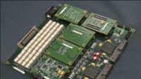
Embedded Technology
32-bit Microprocessor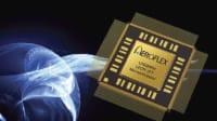
Top Stories
INSIDERManufacturing & Prototyping
![]() How Airbus is Using w-DED to 3D Print Larger Titanium Airplane Parts
How Airbus is Using w-DED to 3D Print Larger Titanium Airplane Parts
INSIDERManned Systems
![]() FAA to Replace Aging Network of Ground-Based Radars
FAA to Replace Aging Network of Ground-Based Radars
NewsTransportation
![]() CES 2026: Bosch is Ready to Bring AI to Your (Likely ICE-powered) Vehicle
CES 2026: Bosch is Ready to Bring AI to Your (Likely ICE-powered) Vehicle
NewsSoftware
![]() Accelerating Down the Road to Autonomy
Accelerating Down the Road to Autonomy
EditorialDesign
![]() DarkSky One Wants to Make the World a Darker Place
DarkSky One Wants to Make the World a Darker Place
INSIDERMaterials
![]() Can This Self-Healing Composite Make Airplane and Spacecraft Components Last...
Can This Self-Healing Composite Make Airplane and Spacecraft Components Last...
Webcasts
Defense
![]() How Sift's Unified Observability Platform Accelerates Drone Innovation
How Sift's Unified Observability Platform Accelerates Drone Innovation
Automotive
![]() E/E Architecture Redefined: Building Smarter, Safer, and Scalable...
E/E Architecture Redefined: Building Smarter, Safer, and Scalable...
Power
![]() Hydrogen Engines Are Heating Up for Heavy Duty
Hydrogen Engines Are Heating Up for Heavy Duty
Electronics & Computers
![]() Advantages of Smart Power Distribution Unit Design for Automotive...
Advantages of Smart Power Distribution Unit Design for Automotive...
Unmanned Systems
![]() Quiet, Please: NVH Improvement Opportunities in the Early Design...
Quiet, Please: NVH Improvement Opportunities in the Early Design...