


Radiation Effects on Electronics in Aligned Carbon Nanotube Technology (RadCNT)
Characterizing the fundamental mechanisms and charge transport phenomena governing the interactions between ionizing and non-ionizing radiation with carbon-based (nanotube and graphene) field-effect transistors (FETs) devices and integrated circuits (ICs).
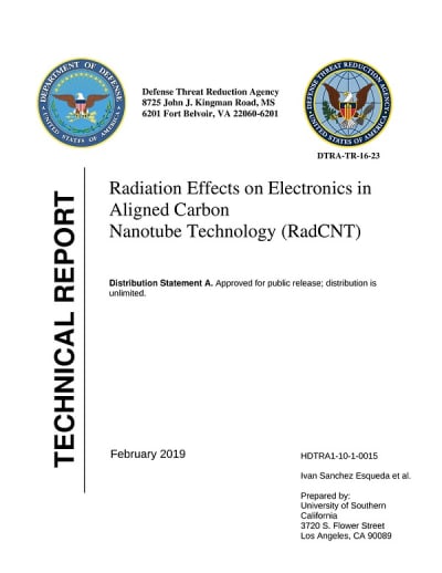
The main objective of the RadCNT program was the characterization of fundamental mechanisms and charge transport phenomena governing the interactions between ionizing and non-ionizing radiation with carbon-based (nanotube and graphene) field-effect transistors (FETs) devices and integrated circuits (ICs). This effort was supported through the fabrication of aligned single-walled carbon nanotubes (SWCNT) FETs at the University of Southern California’s (USC) Nanotechnology Research Laboratory and through a collaboration with the Naval Research Laboratories (NRL) for radiation testing and expertise in radiation effects characterization.

The RadCNT program concentrated on understanding total ionizing dose (TID) effects on SWCNT and graphene FETs. Several TID experiments with SWCNT and graphene FETs with various gate configurations, dielectric materials and geometries were performed as part of this effort. Well-known mechanisms of radiation-induced degradation in FETs such as oxide charge buildup were confirmed in SWCNT and graphene FETs through in situ measurements following radiation exposure. The effects of ionizing radiation on charge-injection mechanisms that cause gate hysteresis in carbon-based electronics were also investigated and demonstrated experimentally for the first time in aligned SWCNT FETs.
Total ionizing dose (TID) experiments were performed in view of initial investigations in carbon-based electronics devices (both SWCNT and graphene FETs) that reported a strong dependence of the radiation response on the experimental environment. These experiments consisted of Co-60 gamma ray irradiation of aligned single-walled carbon nanotube (SWCNT) field effect transistors (FETs) fabricated with 30 nm Al2O3 gate dielectrics and individual back gate electrodes.
Results indicate net positive voltage shifts in the transfer (Id–Vgs) characteristics of FETs fabricated without a passivation layer masking the surface of the device (i.e., having the SWCNTs exposed to the testing environment). The measured shifts are attributed to contaminants that alter the condition at the surface of the device resulting in an effective p-type doping of the nanotubes. These results are consistent with previous investigations where molecular adsorption at the surface of the SWC-NTs and/or at the SiO2 surface near the CNTs results in electron traps that can modulate the nanotube carrier density when irradiated in air. On the other hand, devices fabricated with a passivation layer (i.e., 1 μm thick coating of 3612 photoresist) resulted in net negative voltage shifts characteristic of positive charge trapping in the oxide near the SWCNT/oxide interface.
The impact of ionizing radiation on charge injection mechanisms was established experimentally through in situ measurements of SWCNT FETs performed under static vacuum. Extractions of hysteresis width (h) indicated an increase of more than 20 % after 1 Mrad(SiO2) of TID exposure for worst-case conditions. This increase in h indicates a larger contribution from charge injection mechanisms as a function of ionizing radiation exposure. TCAD simulations were used to investigate the combined effect of hysteresis and radiation-induced degradation and to demonstrate its dependence on trap density, carrier lifetime and energy distribution.
The measurements of hysteresis as a function of increasing radiation exposure and gate voltage (Vg) sweep range reveal non-uniform buildup in the energy distribution of trapping centers near the SWCNT/dielectric interface. The results are consistent with extensive studies on classical bulk semiconductor/oxide interfaces (e.g., in the Si/SiO2 system).
TID experiments on graphene FETs were also performed as part of the Rad-CNT program. Graphene FETs fabricated by chemical vapor deposition (CVD) and transferred onto trimethylsiloxy (TMS)-passivated SiO2Si substrates and epitaxial graphene on 6H-SiC substrates (via Si sublimation) had similar TID responses. In both cases radiation exposure resulted in positive oxide trapped charges near the graphene/oxide interface as manifested by negative voltage shifts in the Id-Vgs characteristics, degradation of carrier mobilities and increased minimum conductivity.
A semi-empirical approach for modeling the radiation-induced degradation effective carrier mobility in graphene FETs was also developed as part of this effort. The modeling approach describes Coulomb and short-range scattering based on calculations of charge and electric field that incorporate radiation-induced oxide trapped charges. The model can correctly describe the transition of the dominant scattering mechanism as a function of effective vertical field and oxide trapped charge density. The proposed modeling approach was verified with experimental data from Co-60 irradiation of graphene FETs resulting in excellent qualitative agreement.
This work was done by Ivan Sanchez Esqueda, Cory D. Cress, Chongwu Zhou, Yuchi Che, Yue Fu, and Jonathan Ahlbin of the University of Southern California for the Defense Threat Reduction Agency. For more information, download the Technical Support Package (free white paper) below. DTRA-0011
This Brief includes a Technical Support Package (TSP).
Radiation Effects on Electronics in Aligned Carbon Nanotube Technology (RadCNT)
(reference DTRA-0011) is currently available for download from the TSP library.
Don't have an account?
More From SAE Media Group

Tech Briefs
Fabricating Nanochips via Thermal Lithography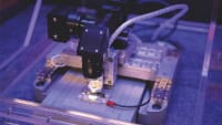
Tech Briefs
How to Make a Transistor – From Thread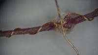
Tech Briefs
Rolled 2D Heterostructures
Electronics & Sensors INSIDER
Researchers Wire Up Individual Graphene Nanoribbons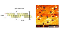

Electronics & Sensors INSIDER
Researchers Create First Functional Semiconductor Made from Graphene
Tech Briefs
Graphene “Nano-Origami” Creates Tiny Microchips
Electronics & Sensors INSIDER
Tiny But Mighty: Next-Gen Transistors Hold Great Promise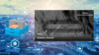

Tech Briefs
Coating Protects Fragile Quantum Electronics

Medical Design Briefs
Atomic Chains in Nanotubes Push the Electronics Frontier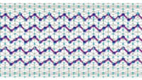
Advanced Manufacturing INSIDER
Computer Chip Manufacturing Method Squeezes More onto Wafers
Electronics & Sensors INSIDER
Innovative Technique Could Pave the Way for New Generation of Flexible Electronic Components
Electronics & Sensors INSIDER
Leading Experts Suggest Guidelines for Assessing Emerging Transistor Performance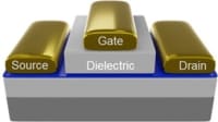
Electronics & Sensors INSIDER
MIT Team Takes a Major Step Toward Fully 3D-Printed Active Electronics
Tech Briefs
Integrating Fragile 2D Materials into Devices
Tech Briefs
Sandwiching Materials in Nanoelectronics
Photonics & Imaging Technology
Individual Quantum Dots Imaged in 3-D for the First Time
Electronics & Sensors INSIDER
2D Materials for Extra Thin Computer Chips
Embedded Computing INSIDER
Researchers Create Smallest Transistor Ever

Electronics & Sensors INSIDER
This Advance May Enable 2D Transistors for Tinier Microchip Components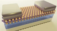
Motion Design INSIDER
New Transfer Process Moves 2D Materials from Growth Substrate to Device Substrate
Electronics & Sensors INSIDER
Atomic Scale Semiconductor Chips — Pushing the Limits
Electronics & Sensors INSIDER
Graphene-Based Electronics


Overview
The document is a technical report titled "Radiation Effects on Electronics in Aligned Carbon Nanotube Technology (RadCNT)," authored by Ivan Sanchez Esqueda and Cory D. Cress, covering the period from March 22, 2010, to March 21, 2013. The primary objective of the RadCNT program was to investigate the fundamental mechanisms and charge transport phenomena that govern the interactions between ionizing and non-ionizing radiation with carbon-based field-effect transistors (FETs) and integrated circuits (ICs).
The research was conducted at the University of Southern California’s Nanotechnology Research Laboratory, with significant collaboration from the Naval Research Laboratories (NRL) for radiation testing and expertise in characterizing radiation effects. The program focused on understanding the total ionizing dose (TID) effects on single-walled carbon nanotube (SWCNT) and graphene FETs. Various experiments were performed to assess the impact of TID on these devices, utilizing different gate configurations, dielectric materials, and geometries.
The report outlines the experimental setup, including the test structures used and the methodologies employed to evaluate the radiation effects on the carbon-based FETs. It details the results obtained from the experiments, highlighting the performance and reliability of SWCNT and graphene FETs under radiation exposure. The findings contribute to a deeper understanding of how these advanced materials behave in radiation environments, which is crucial for their application in space and military electronics.
Additionally, the report discusses future work and potential improvements in the design and fabrication of carbon-based electronic devices to enhance their resilience against radiation. It emphasizes the importance of continued research in this area to develop robust technologies that can withstand harsh conditions.
The document also includes sections on recent accomplishments, participating organizations, and the impact of the research, showcasing the collaborative efforts and advancements made during the program. Overall, the RadCNT program represents a significant step forward in the field of radiation effects on electronics, particularly in the context of carbon nanotube technology, with implications for various applications in defense and aerospace sectors.
Top Stories
INSIDERManned Systems
![]() How Airbus is Using w-DED to 3D Print Larger Titanium Airplane Parts
How Airbus is Using w-DED to 3D Print Larger Titanium Airplane Parts
INSIDERAerospace
![]() FAA to Replace Aging Network of Ground-Based Radars
FAA to Replace Aging Network of Ground-Based Radars
NewsUnmanned Systems
![]() Microvision Aquires Luminar, Plans Relationship Restoration, Multi-industry Push
Microvision Aquires Luminar, Plans Relationship Restoration, Multi-industry Push
NewsDesign
![]() CES 2026: Bosch is Ready to Bring AI to Your (Likely ICE-powered) Vehicle
CES 2026: Bosch is Ready to Bring AI to Your (Likely ICE-powered) Vehicle
NewsSoftware
![]() Accelerating Down the Road to Autonomy
Accelerating Down the Road to Autonomy
INSIDERManned Systems
![]() Can This Self-Healing Composite Make Airplane and Spacecraft Components Last...
Can This Self-Healing Composite Make Airplane and Spacecraft Components Last...
Webcasts
Power
![]() Hydrogen Engines Are Heating Up for Heavy Duty
Hydrogen Engines Are Heating Up for Heavy Duty
Transportation
![]() Advantages of Smart Power Distribution Unit Design for Automotive...
Advantages of Smart Power Distribution Unit Design for Automotive...
Automotive
![]() Quiet, Please: NVH Improvement Opportunities in the Early Design...
Quiet, Please: NVH Improvement Opportunities in the Early Design...
Power
![]() A FREE Two-Day Event Dedicated to Connected Mobility
A FREE Two-Day Event Dedicated to Connected Mobility
Connectivity
![]() E/E Architecture Redefined: Building Smarter, Safer, and Scalable Vehicles
E/E Architecture Redefined: Building Smarter, Safer, and Scalable Vehicles
Manufacturing & Prototyping
![]() How Sift's Unified Observability Platform Accelerates Drone Innovation
How Sift's Unified Observability Platform Accelerates Drone Innovation