


Direct-Write Polymer Nanolithography in Ultra-High Vacuum
Deposition of materials in vacuum is essential to minimizing defects in electronic circuits.
The deposition of materials in vacuum is the foundational technology for creating modern electronic circuits; a vacuum being essential both to preserve the cleanliness of the substrate and the deposited materials, and to minimize the creation of defects. Consequently, most deposition techniques, from thermal evaporation to atomic layer deposition, require a high level of vacuum, preferably ultra-high vacuum (UHV), to be used effectively.
To date, additive lithographies such as inkjet, dip-pen nanolithography (DPN), and micro-contact printing have been limited to deposition under ambient pressures, and therefore cannot achieve the benefits of the controlled environment under vacuum. One type of additive lithography is scanning probe lithography (SPL), where sharp probes either guide the deposition of material to a substrate, or modify previously deposited films. In the case of DPN, the atomic force microscopy (AFM) probe can be used to write a wide range of molecular inks with resolutions down to 15 nm. However, in conventional DPN, writing depends on the intrinsic fluidity of the ink molecules or on the creation of ink fluidity using solvents. Unfortunately, inks and solvents that have sufficient intrinsic fluidity for DPN evaporate quickly in vacuum.
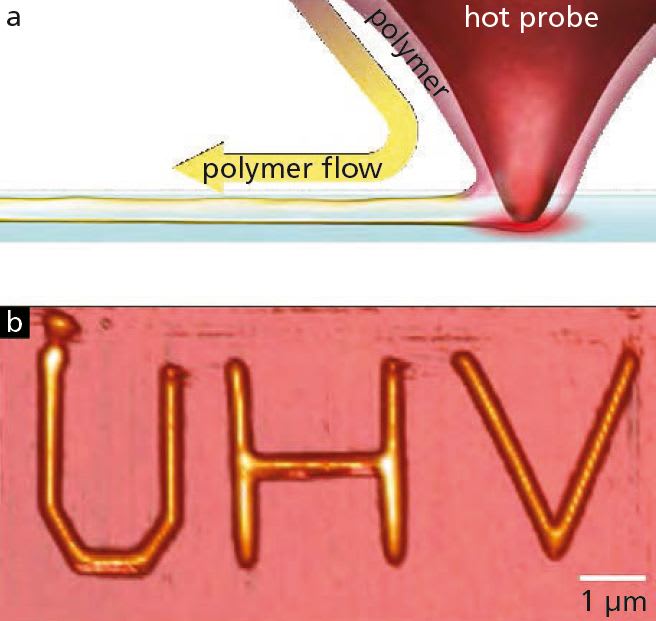
This work demonstrates that thermal dip-pen nanolithography (tDPN) can deposit polymer nanostructures from a heated AFM tip in a high-vacuum environment. In tDPN, the probe temperature may be varied precisely within microseconds over a temperature range of 1000 °C. The probe temperature controls the viscosity of the coated ink, allowing independent control over the overall deposition rate, and the ability to turn off and on deposition. Many different materials, nanoparticles, and SAM molecules have been deposited using this technique.
Thermal DPN closely mirrors the capabilities of conventional DPN, but with greater control over the ink flow. Critically, the heat from the probes enables the deposition of high-meltingpoint inks such as polymers that also have low volatility and so may be deposited under a vacuum.
The initial approach for depositing organic inks was to attempt DPN with octadecanethiol (ODT), a classic ink for DPN that reproducibly transfers to the substrate. However, it was found that the ink on the DPN tip would invariably evaporate in the load lock chamber (~10-7 Torr), leaving insufficient coverage for observable deposition. Evaporation is readily observed visually since the ink leaves a haze on the tip that is absent after placing in a load lock chamber. This observation was more rigorously examined by creating a sample that mimicked the DPN tip surface chemistry: A silicon oxide on a silicon chip that was coated by holding it over ODT in a scintillation vial heated to 65 °C for 30 minutes. This procedure produced an ODT film that was 20-nm thick (measured by ellipsometry).
After placing the chip briefly under vacuum in a load lock chamber (~10-7 Torr), no ODT film was detectable. Additional attempts with less volatile inks — such as eicosanethiol — yielded similar results, leading to the conclusion that typical inks used in conventional DPN cannot be used for DPN under vacuum.
While alkanethiols could not be deposited, it was found that heated probes would retain and deposit polymer in UHV. For this work, the polymer to be poly(3-dodecylthiophene) (PDDT) was chosen, a conducting polymer that has found widespread usage in organic electronics. The probe temperature was controlled by applying current through the probe heater. One of the advantages of UHV tDPN is the lower melting point of inks under UHV. Because the molar volume of PDDT is lower in solid form than in liquid form, thermodynamics indicate that its melting point should drop as the surrounding pressure is lowered. The lower deposition temperature also reduces the risk of thermal damage when applied to prefabricated devices.
The molecular structure of the written PDDT monolayer nanostructure films depends on the chemistry of the silicon surface. Oxide termination leads to polymer side chains aligning perpendicular to the substrate, whereas silicon termination leads to the polymer lying flat. The thickness of the deposited polymer is a function of the speed of the scanning probe, and may be controlled monolayer-by-monolayer.
This new UHV-compatible direct-write technique should be of value both for nanoscale lithography of polymer structures and for the study of molecularly ordered polymer nanostructures. This result would also open a new method of studying polymer-semiconductor surface interaction at a molecular level, which is useful to develop polymer-based electronics compatible with inorganic semiconductor technology.
This work was done by Woo-Kyung Lee, Arnaldo R. Laracuente, and Paul E. Sheehan of the Naval Research Laboratory; Minchul Yang of the US Patent and Trademark Office; William P. King of the University of Illinois Urbana-Champaign; and Lloyd J. Whitman of the National Institute for Science and Technology. NRL-0059
This Brief includes a Technical Support Package (TSP).
Direct-Write Polymer Nanolithography in Ultra-High Vacuum
(reference NRL-0059) is currently available for download from the TSP library.
Don't have an account?
More From SAE Media Group
Aerospace & Defense Tech Briefs
How to Select the Right Silicone for Space Applications
Tech Briefs
Self-Healing, Highly Adhesive Elastomers
Medical Design Briefs
3D Printable Polymer Nanocomposite Ink
Medical Design Briefs
Transforming Plastic Parts into High-Value Products
Medical Design Briefs
Plasma Treatment: Transforming Plastic Parts into High-Value Products
Aerospace & Defense Tech Briefs
Design of New Piezoelectric Composites Using Nanocellulose
Tech Briefs
Self-Healing, Recyclable, Shape Memory Polymers
Medical Design Briefs
New Material Family Could Build Realistic Prosthetics
Tech Briefs
Conductive Carbon Fiber Polymer Composite
Tech Briefs
Miniscule Robots of Metal and Plastic
Tech Briefs
High-Color-Purity 3D Printing

Medical Design Briefs
Streamlining Medical Device Development and Manufacturing Using Silicone Elastomers
Medical Design Briefs
Medical Plastics: Understanding Ultrasonic Welding, Part 1

Tech Briefs
Method Sprays Extremely Thin Wires on 3D Objects
Medical Design Briefs
What Medical Device OEMs Should Know About Outsourced MIM
Tech Briefs
Organic Material for Printed Electronics
Tech Briefs
Fiber-Metal Laminate Manufacturing Technique
Tech Briefs
3D Printing with an Unknown Material
Tech Briefs
Automated Tow/Tape Placement System
Tech Briefs
3D-Printed Composites for High-Temperature Uses
Tech Briefs
3D Printing of All-Liquid 3D Structures
Tech Briefs
Precision CNT Cutting Mechanism
Aerospace & Defense Tech Briefs
‘Nanostitches’ Enable Lighter and Tougher Composite Materials
Overview
The document presents a study on direct-write polymer nanolithography conducted in ultra-high vacuum (UHV) conditions, published in the Beilstein Journal of Nanotechnology. The research focuses on a novel method for creating polymer nanostructures on substrates using atomic force microscope (AFM) probes that are heated to control the viscosity of the polymer ink. This technique allows for precise deposition of materials, which is crucial for the fabrication of modern electronic circuits.
The authors, including Woo-Kyung Lee and Paul E. Sheehan, highlight the importance of maintaining a high level of vacuum during the deposition process to ensure the cleanliness of both the substrate and the deposited materials, thereby minimizing defects. Traditional deposition methods often require multiple steps, but this additive lithography approach enables the direct placement of material in the desired location in a single step.
The study details how the writing speed of the AFM tip can be adjusted to control the number of polymer ink monolayers deposited on the surface, ranging from a single layer to multiple layers. Higher writing speeds result in thinner nanostructures, which can be tailored for specific applications. The research also explores the effects of different substrate materials on the orientation of the polymer chains. For instance, deposition on silicon oxide-terminated substrates leads to upright polymer chains, while vacuum-reconstructed silicon surfaces result in aligned chains.
The findings indicate that the ability to control deposition temperature and conditions in UHV not only enhances the precision of the nanostructures but also reduces the risk of thermal damage to pre-fabricated devices. The temperature window between melting and thermal decomposition of the polymer, specifically PDDT, is widened, allowing for greater control over the characteristics of the deposited structures.
Overall, this research contributes to the field of nanotechnology by providing a method for creating high-quality polymer nanostructures with potential applications in electronics and other advanced materials. The study emphasizes the significance of UHV conditions in achieving precise and defect-free material deposition, which is essential for the development of next-generation electronic devices.
Top Stories
INSIDERManufacturing & Prototyping
![]() How Airbus is Using w-DED to 3D Print Larger Titanium Airplane Parts
How Airbus is Using w-DED to 3D Print Larger Titanium Airplane Parts
INSIDERManned Systems
![]() FAA to Replace Aging Network of Ground-Based Radars
FAA to Replace Aging Network of Ground-Based Radars
NewsTransportation
![]() CES 2026: Bosch is Ready to Bring AI to Your (Likely ICE-powered) Vehicle
CES 2026: Bosch is Ready to Bring AI to Your (Likely ICE-powered) Vehicle
NewsSoftware
![]() Accelerating Down the Road to Autonomy
Accelerating Down the Road to Autonomy
EditorialDesign
![]() DarkSky One Wants to Make the World a Darker Place
DarkSky One Wants to Make the World a Darker Place
INSIDERMaterials
![]() Can This Self-Healing Composite Make Airplane and Spacecraft Components Last...
Can This Self-Healing Composite Make Airplane and Spacecraft Components Last...
Webcasts
Defense
![]() How Sift's Unified Observability Platform Accelerates Drone Innovation
How Sift's Unified Observability Platform Accelerates Drone Innovation
Automotive
![]() E/E Architecture Redefined: Building Smarter, Safer, and Scalable...
E/E Architecture Redefined: Building Smarter, Safer, and Scalable...
Power
![]() Hydrogen Engines Are Heating Up for Heavy Duty
Hydrogen Engines Are Heating Up for Heavy Duty
Electronics & Computers
![]() Advantages of Smart Power Distribution Unit Design for Automotive...
Advantages of Smart Power Distribution Unit Design for Automotive...
Unmanned Systems
![]() Quiet, Please: NVH Improvement Opportunities in the Early Design...
Quiet, Please: NVH Improvement Opportunities in the Early Design...